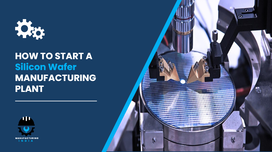
Starting a silicon wafer manufacturing plant can be a highly lucrative and technologically advanced business venture given the explosive global demand for semiconductors, electronics, and renewable energy technologies. Silicon wafers are the fundamental building blocks of the modern digital economy, serving as the substrate for integrated circuits, microprocessors, solar cells, and countless electronic devices. This comprehensive guide will walk you through every step of establishing your silicon wafer manufacturing business.
Market Overview
The silicon wafer industry is experiencing unprecedented growth worldwide as digital transformation accelerates across all sectors of the economy. Silicon wafers are the essential foundation for semiconductor chips that power smartphones, computers, automobiles, industrial equipment, artificial intelligence systems, and renewable energy infrastructure. The global silicon wafer market reached approximately twelve point five billion USD in twenty twenty-three and is projected to exceed eighteen billion USD by twenty thirty, driven by surging demand from the semiconductor industry, explosive growth in solar energy adoption, advancement of five G networks and Internet of Things devices, expansion of electric vehicles and automotive electronics, and increasing deployment of artificial intelligence and edge computing technologies. With proper planning, substantial capital investment, and commitment to quality excellence, a silicon wafer manufacturing plant can achieve exceptional profitability while participating in the technological revolution shaping our future.
Step 1: Conduct Comprehensive Market Research and Feasibility Analysis
Before committing to the substantial investment required for a silicon wafer manufacturing plant, thorough market research and feasibility analysis are absolutely essential. Analyze the demand patterns for different wafer sizes including legacy one hundred millimeter and one hundred fifty millimeter wafers for specialized applications, two hundred millimeter wafers for automotive and power electronics, and three hundred millimeter wafers for advanced logic and memory chips. Identify your target customer segments including semiconductor fabrication facilities, solar cell manufacturers, micro-electromechanical systems producers, power electronics companies, and research institutions. Study the competitive landscape including established global manufacturers, regional players, and emerging competitors to understand their technology capabilities, pricing strategies, quality standards, and market positioning. Evaluate the availability and reliability of polysilicon suppliers, as securing high-purity feedstock is critical for operations. Assess regional advantages such as proximity to semiconductor clusters, availability of ultrapure water sources, reliable electrical infrastructure, and access to skilled technical workforce. Analyze export opportunities particularly to high-growth markets in Asia, North America, and Europe where semiconductor demand continues expanding rapidly.
Step 2: Develop Detailed Business Plan and Technology Strategy For Silicon Wafer Manufacturing Plant
A comprehensive business plan serves as your strategic roadmap and is essential for securing financing. Define your business objectives clearly including target production capacity measured in wafers per month, wafer size focus such as two hundred millimeter or three hundred millimeter, product specialization including polished wafers, epitaxial wafers, or silicon-on-insulator products, and quality tier targeting commodity, standard, or premium segments. Outline your technology approach including crystal growing methodology such as Czochralski or float zone processes, automation level from semi-automated to fully automated production lines, and equipment sourcing strategy balancing new versus refurbished machinery. Develop comprehensive financial projections covering initial capital investment ranging from fifteen million to over one hundred million USD depending on scale, monthly operating expenses including raw materials, utilities, labor, and maintenance, revenue forecasts based on realistic capacity utilization ramps, and detailed break-even analysis. Your business plan should address critical risks including rapid technology evolution requiring equipment upgrades, cyclical nature of semiconductor demand, intense competition from established manufacturers, and environmental compliance requirements along with mitigation strategies for each risk factor.
Step 3: Secure Regulatory Approvals and Environmental Clearances
Establishing a silicon wafer manufacturing plant requires navigating complex regulatory requirements given the industry’s environmental impact and technical complexity. Register your business entity choosing an appropriate structure such as private limited company or corporation based on your investment scale and ownership structure. Obtain industrial manufacturing licenses from relevant state or regional industrial development authorities. Apply for comprehensive environmental clearances from pollution control boards addressing air emissions from furnaces and chemical processes, wastewater discharge from cleaning and etching operations, hazardous waste management for chemical residues and reject materials, and noise control for mechanical equipment. Secure chemical storage and handling licenses for hazardous materials including hydrofluoric acid, sulfuric acid, nitric acid, and hydrogen peroxide. Obtain electrical safety certifications for high-voltage equipment and power infrastructure. Register for appropriate tax identifications and comply with import-export regulations if sourcing equipment internationally or exporting products. Depending on your target markets, plan for quality management system certifications such as ISO nine thousand and one, environmental management certification ISO fourteen thousand and one, and occupational health and safety certification ISO forty-five thousand and one which are increasingly expected by major semiconductor customers.
Step 4: Arrange Substantial Financing and Investment Capital
Silicon wafer manufacturing requires significant capital investment, making financing arrangement a critical early step. Determine your total capital requirement comprehensively including land acquisition typically two to five acres for medium-scale facility, specialized building construction with clean room infrastructure, comprehensive machinery and equipment suite, ultra-pure water treatment systems, chemical distribution infrastructure, electrical power systems including backup generation, initial raw material inventory particularly polysilicon, and adequate working capital for six to twelve months of operations. For a two hundred millimeter wafer facility producing fifty thousand to two hundred thousand wafers monthly, expect total investment between fifteen million and fifty million USD. For a three hundred millimeter facility producing one hundred thousand to five hundred thousand wafers monthly, total investment ranges from thirty million to over one hundred million USD. Explore diverse financing sources including commercial bank loans secured by assets and guaranteed by promoters, government incentives and subsidies for semiconductor and renewable energy industries, strategic partnerships with semiconductor companies seeking secure wafer supply, private equity investors attracted to high-technology manufacturing, and venture capital for innovative processing technologies. Prepare detailed project reports with technical specifications, equipment lists, process flow diagrams, financial projections, and market analysis to present to financial institutions and investors. Many governments worldwide offer attractive incentives for semiconductor industry development given its strategic importance.
Request a Sample Report for In-Depth Market Insights: https://www.imarcgroup.com/silicon-wafer-manufacturing-plant-project-report/requestsample
Step 5: Select Optimal Location with Critical Infrastructure
Location selection profoundly impacts operational success given the stringent requirements of silicon wafer manufacturing. Choose a site within established industrial zones or semiconductor parks offering industrial infrastructure and regulatory support. Ensure absolutely reliable electrical power supply with at least ninety-nine point nine percent uptime, as power interruptions can ruin entire crystal growing batches costing hundreds of thousands of dollars. The location must provide access to abundant high-quality water sources for ultra-pure water production, as wafer cleaning consumes enormous quantities. Verify excellent transportation connectivity for receiving polysilicon shipments, chemical deliveries, and distributing finished wafers to customers. Consider proximity to semiconductor fabrication clusters to minimize logistics costs and strengthen customer relationships. The site must comply with industrial and environmental zoning regulations while being sufficiently distant from residential areas given chemical usage. Ensure availability of technical workforce or proximity to technical universities for recruitment. Assess seismic stability as vibrations affect crystal growing and precision processes. Plan for adequate land area accommodating crystal growing rooms, slicing and processing areas, clean room facilities, chemical storage, wastewater treatment, warehousing, and future expansion. The location should provide reliable telecommunications infrastructure for process monitoring and customer communication.
Step 6: Design and Construct Specialized Manufacturing Facility
Silicon wafer manufacturing demands highly specialized facility design meeting exacting standards. Plan your facility layout optimizing production flow from raw polysilicon to packaged wafers. Designate separate controlled areas for crystal growing rooms requiring vibration isolation and precise temperature control, ingot preparation and slicing sections with adequate ventilation for silicon dust, wet processing areas for etching and cleaning with chemical-resistant construction, clean room zones for polishing and inspection meeting ISO Class four or five standards, metrology and quality control laboratories with environmental isolation, chemical storage facilities with secondary containment and safety systems, ultra-pure water production and distribution, wastewater treatment plant, finished goods storage with climate control, and administrative offices. The crystal growing area requires exceptional vibration isolation achieved through special foundation design and isolation from other operations. Clean room construction is the most expensive component, costing three thousand to ten thousand USD per square meter, incorporating HEPA filtration systems achieving ninety-nine point nine seven percent particle removal, precise temperature control maintaining twenty to twenty-two degrees Celsius plus or minus half degree, humidity control at forty to forty-five percent relative humidity plus or minus two percent, and positive air pressure preventing contamination ingress. Install comprehensive safety systems including chemical leak detection and containment, fire suppression systems appropriate for chemical fires, emergency eyewash and shower stations, exhaust and scrubber systems for chemical fumes, and emergency power backup for critical systems. Design efficient material flow paths minimizing contamination risks and handling damage.
Step 7: Procure Advanced Machinery and Processing Equipment
The machinery investment represents the largest capital component and determines your production capability and quality level. Essential equipment for silicon wafer manufacturing includes crystal growing equipment such as Czochralski pullers costing five hundred thousand to two million USD each for producing silicon ingots, with larger diameter capabilities commanding premium prices. Acquire multiple pullers to ensure continuous production and provide redundancy. Procure diamond wire slicing machines costing three hundred thousand to one point five million USD per unit for cutting ingots into individual wafers, with multi-wire systems processing multiple ingots simultaneously. Invest in edge grinding machines costing one hundred thousand to four hundred thousand USD for rounding wafer edges and preventing chipping. Purchase double-sided lapping systems costing two hundred thousand to eight hundred thousand USD for achieving precise thickness uniformity across wafer surfaces. Acquire chemical etching systems costing one hundred fifty thousand to five hundred thousand USD for removing surface damage and creating desired surface characteristics. Invest substantially in chemical mechanical polishing equipment costing four hundred thousand to two million USD per system for achieving mirror-finish surfaces with sub-nanometer roughness critical for semiconductor applications. For specialized products, consider epitaxial reactors costing one million to five million USD for depositing crystalline silicon layers with precise thickness and doping control. Procure comprehensive metrology and inspection equipment costing collectively one to five million USD including optical surface scanners, resistivity testers, thickness measurement systems, flatness analyzers, and particle detection systems. Invest in automated material handling systems including wafer transfer robots and automated guided vehicles to minimize human contact and contamination. Purchase ultra-pure water systems costing five hundred thousand to two million USD producing water with resistivity exceeding eighteen megohm-centimeter. Install chemical distribution systems with automated delivery and monitoring. Select equipment carefully balancing capability, reliability, automation level, and cost while ensuring compatibility and integration across the production line.
Step 8: Establish Reliable Polysilicon Supply Chain
Securing consistent supply of high-purity polysilicon is absolutely critical for sustainable operations, as raw material represents thirty to forty percent of production costs. Establish relationships with reputable polysilicon manufacturers who can consistently deliver semiconductor-grade material with purity exceeding ninety-nine point nine nine nine nine nine nine nine percent, commonly called nine-N purity. Evaluate suppliers based on quality consistency, production capacity, financial stability, and willingness to enter long-term supply agreements. Consider contracting with multiple suppliers to mitigate supply disruption risks and negotiate favorable pricing. Understand that polysilicon pricing fluctuates significantly with market conditions, ranging from fifteen to over fifty USD per kilogram depending on supply-demand dynamics and geopolitical factors. Negotiate long-term contracts with price stabilization mechanisms when possible, though suppliers may resist fixed pricing given their own silicon feedstock cost volatility. Plan for adequate polysilicon inventory maintaining at least one to three months of production requirements, though excessive inventory ties up capital and risks price depreciation. Implement rigorous incoming quality control testing including purity verification through mass spectrometry or other analytical techniques, physical inspection for contamination, and documentation review ensuring traceability. Consider strategic partnerships with polysilicon producers potentially involving equity participation or take-or-pay commitments in exchange for guaranteed supply and favorable pricing. Monitor global polysilicon market dynamics closely as supply constraints or oversupply situations dramatically impact your raw material costs and overall profitability.
Step 9: Recruit and Train Highly Skilled Technical Workforce
Silicon wafer manufacturing requires a specialized workforce combining materials science knowledge, process engineering expertise, and precision manufacturing skills. Recruit experienced personnel for critical roles including plant manager with semiconductor manufacturing background, crystal growing engineers expert in Czochralski or float zone processes, process engineers for slicing, polishing, and cleaning operations, metrology and quality control specialists with analytical chemistry and materials characterization expertise, equipment maintenance engineers familiar with complex semiconductor tools, clean room technicians trained in contamination control protocols, environmental health and safety officers knowledgeable in chemical handling and semiconductor industry standards, and production operators capable of running sophisticated automated equipment. For a medium-scale facility, expect to employ fifty to two hundred people depending on automation level. Provide comprehensive training programs covering silicon crystal growth fundamentals and troubleshooting, wafer slicing techniques minimizing kerf loss and surface damage, chemical etching and cleaning procedures with emphasis on safety, chemical mechanical polishing process optimization, metrology techniques and statistical process control, clean room protocols and contamination control, equipment operation and preventive maintenance, quality standards and defect classification, workplace safety especially chemical handling, and environmental compliance procedures. Partner with semiconductor industry associations, technical universities, or equipment suppliers for specialized training programs. Consider sending key personnel to established wafer manufacturers or equipment vendor training centers. Implement continuous skill development ensuring your team stays current with evolving technologies and best practices. Establish a strong safety culture given the hazardous chemicals and high-temperature processes involved. Competitive compensation and career development opportunities are essential for retaining skilled personnel in this specialized industry.
Step 10: Implement Rigorous Crystal Growing and Processing Protocols
The crystal growing process fundamentally determines wafer quality and production economics, requiring meticulous control and optimization. Implement standardized procedures for Czochralski crystal growing beginning with loading ultra-pure polysilicon chunks into quartz crucibles, adding precise dopant quantities for desired electrical properties such as boron for P-type or phosphorus for N-type wafers, heating silicon to melting point around fourteen hundred twenty degrees Celsius in inert argon atmosphere, dipping seed crystal into molten silicon and establishing initial crystallization, and slowly pulling seed upward at carefully controlled rate typically point five to two millimeters per minute while rotating to achieve cylindrical shape and uniform properties. Monitor critical parameters continuously including melt temperature with precision better than one-tenth degree, pull rate affecting crystal diameter and quality, rotation speeds of crystal and crucible, and chamber pressure and gas flow. A single crystal growing run takes twenty-four to forty-eight hours producing one to two meter long ingots. After cooling, inspect ingots for crystal defects using X-ray diffraction and visual examination. Implement precise ingot shaping procedures grinding ingots to exact diameter specifications, creating flat or notch orientation markers, and removing unusable crown and tail sections. Execute wafer slicing using diamond wire saws with meticulous tension control minimizing kerf loss while achieving target thickness, typically two hundred to eight hundred micrometers depending on application. Implement careful edge grinding rounding wafer periphery with typical radius one hundred fifty to two hundred fifty micrometers preventing edge chips during subsequent handling. Conduct lapping operations removing saw damage and achieving thickness uniformity within two to five micrometers across entire wafer surface. Perform chemical etching removing subsurface damage layer and preparing surface for polishing. Execute chemical mechanical polishing achieving mirror finish with surface roughness below half nanometer critical for semiconductor device fabrication. Throughout processing, maintain rigorous cleanliness preventing particle contamination that creates defects. Document all process parameters enabling traceability and continuous improvement.
Step 11: Establish Comprehensive Quality Control and Testing Systems
Quality assurance is paramount in silicon wafer manufacturing as even minor defects render wafers unusable for advanced semiconductor applications where customers demand near-perfect quality. Establish a well-equipped metrology laboratory with environmental controls preventing thermal and vibration interference with sensitive measurements. Implement multi-stage quality control beginning with incoming polysilicon verification testing purity through analytical chemistry techniques, inspecting for physical contamination, and reviewing supplier certifications and traceability documentation. Monitor in-process quality during crystal growing measuring ingot diameter continuously, verifying crystal structure and orientation through X-ray diffraction, and testing resistivity confirming proper doping levels. After slicing, inspect every wafer for dimensional accuracy including thickness measured to micrometer precision, diameter meeting specifications, and edge profile within tolerances. Conduct surface quality assessment using automated optical inspection systems detecting particles, scratches, and other surface defects, measuring surface roughness through atomic force microscopy or optical techniques, and evaluating flatness parameters including total thickness variation, bow, and warp. Perform electrical characterization testing resistivity distribution across wafer surface, minority carrier lifetime indicating crystal quality, and surface charge properties. For polished wafers destined for semiconductor manufacturing, customers specify rigorous acceptance criteria including particle density limits often fewer than point one particles per square centimeter for particles above point two micrometers, surface micro-roughness below point five nanometers, flatness specifications typically within few micrometers, and defect density meeting stringent requirements. Implement statistical process control monitoring key parameters and identifying trends before they cause quality excursions. Maintain comprehensive quality records providing full traceability from polysilicon batch through finished wafer lot. Pursue relevant quality certifications including ISO nine thousand and one quality management system demonstrating systematic quality processes, customer-specific qualifications often requiring extensive testing and facility audits, and industry standards such as SEMI specifications for semiconductor wafers. Regular internal audits and continuous improvement initiatives ensure sustained quality performance meeting increasingly demanding customer expectations.
Step 12: Develop Product Portfolio and Customer Specifications
While silicon wafers may appear commodity products, strategic product development and customization create competitive advantages and premium pricing opportunities. Develop a core product portfolio addressing market demands across different wafer sizes with two hundred millimeter wafers for automotive, power electronics, and MEMS applications, and three hundred millimeter wafers for advanced logic, memory, and high-volume semiconductor manufacturing. Offer various product types including polished wafers providing mirror-finish surfaces for standard semiconductor processing, epitaxial wafers featuring deposited crystalline layers for specific device requirements, silicon-on-insulator wafers incorporating buried oxide layers for advanced low-power devices, and annealed wafers with heat treatment for enhanced electrical properties. Provide different doping options including P-type wafers with boron doping for CMOS and power devices, N-type wafers with phosphorus doping for specific applications, and various resistivity ranges from heavily doped to high-resistivity grades. Work closely with customers understanding their specific requirements for flatness tolerances, surface quality specifications, crystal orientation, and contamination limits. Offer customization services such as specific thickness requirements, special edge treatments, custom packaging, and consignment inventory arrangements. Develop application-specific products such as ultra-flat wafers for lithography-intensive processes, high-resistivity wafers for radio-frequency applications, or specific crystal orientations for MEMS devices. Consider vertical product expansion such as reclaimed wafers providing cost-effective substrates for testing and development, or ultra-thin wafers for advanced packaging applications. Product differentiation through superior quality, consistent specifications, and responsive customer service enables premium pricing and customer loyalty in an otherwise commoditized market.
Step 13: Build Strategic Distribution Network and Customer Relationships
Silicon wafer sales operate primarily through direct business-to-business relationships given the technical nature, large transaction values, and quality requirements. Identify and prioritize target customer segments including semiconductor fabrication facilities representing the largest volume market, solar cell manufacturers requiring different specifications at generally lower prices, MEMS and sensor manufacturers needing specialized products, research institutions and universities requiring small volumes of varied specifications, and emerging technology companies developing novel applications. Establish direct sales channels hiring experienced technical sales personnel who understand semiconductor manufacturing and can communicate effectively with customer engineers and procurement teams. Develop long-term supply agreements with major customers providing volume commitments, stable pricing, and dedicated technical support in exchange for guaranteed purchase volumes and multi-year contracts. Such arrangements provide revenue stability and facilitate production planning. Participate actively in semiconductor industry events including SEMICON trade shows, industry conferences, and technical symposiums where you can showcase capabilities, network with potential customers, and stay informed about technology trends and market developments. Develop a professional digital presence with a technical website detailing your capabilities, specifications, and quality systems. Provide comprehensive technical documentation including detailed product specifications, quality certifications, test data, and material safety information. Offer strong customer support including responsive communication, technical consultation, rapid sample provision, and flexibility addressing special requirements. Implement customer qualification processes ensuring potential buyers have legitimate needs and financial stability before extending credit or dedicating production capacity. For international sales, partner with experienced freight forwarders managing export documentation, transportation, and customs clearance for fragile silicon wafers requiring careful handling. Consider regional sales representatives or distributors in key markets, though direct relationships typically yield better margins and customer insights. Build reputation through consistent quality, reliable delivery, and technical competence as word-of-mouth referrals drive significant business in the tight-knit semiconductor community.
Step 14: Implement Robust Environmental Management and Sustainability Practices
Silicon wafer manufacturing involves significant environmental considerations requiring proactive management for regulatory compliance, operational efficiency, and corporate reputation. Implement comprehensive chemical management systems for the numerous hazardous chemicals used in processing including hydrofluoric acid, sulfuric acid, nitric acid, and hydrogen peroxide. Install automated chemical distribution systems minimizing manual handling and exposure risks. Provide secondary containment for chemical storage preventing environmental release in case of spills or leaks. Establish robust wastewater treatment systems as wet processing generates substantial contaminated water requiring treatment before discharge. Install neutralization systems balancing acidic and alkaline waste streams, chemical precipitation removing dissolved metals, filtration systems capturing suspended solids, and polishing treatments achieving discharge standards. Consider water recycling technologies recovering and reusing process water reducing both environmental impact and operational costs. Implement air emission controls including scrubber systems treating exhaust from crystal growing furnaces and chemical processing, removing acid gases, particulates, and organic compounds before atmospheric release. Establish hazardous waste management protocols for reject wafers, spent chemicals, contaminated consumables, and sludge from wastewater treatment. Contract with licensed hazardous waste disposal companies ensuring proper treatment and disposal while maintaining required documentation. Consider silicon reclamation programs recovering value from reject wafers and kerf loss during slicing. Implement energy efficiency measures as silicon wafer manufacturing consumes substantial electrical power, particularly for crystal growing furnaces and clean room environmental controls. Evaluate opportunities for waste heat recovery, efficient motor systems, and optimized process scheduling. Monitor environmental performance through regular testing of air emissions, wastewater discharge, and waste generation. Maintain comprehensive environmental records demonstrating compliance with permits and regulations. Pursue environmental management certification such as ISO fourteen thousand and one demonstrating systematic environmental stewardship. Consider voluntary sustainability initiatives including renewable energy procurement, carbon footprint reduction, and participation in industry sustainability programs. Communicate environmental performance to stakeholders including customers increasingly evaluating suppliers based on environmental criteria, investors interested in environmental, social, and governance factors, and communities concerned about industrial environmental impacts.
Profitability and Growth Potential
The silicon wafer manufacturing business offers attractive profit margins when operated efficiently, particularly given the robust long-term demand outlook driven by digital transformation and renewable energy adoption. Focus on achieving operational excellence through high crystal growing yields minimizing polysilicon waste, optimizing slicing processes reducing kerf loss, maintaining consistently high wafer quality minimizing reject rates, and implementing lean manufacturing principles reducing costs while maintaining quality. Build strong customer relationships through superior quality, reliable delivery, responsive service, and technical collaboration. As your business establishes market presence and demonstrates capabilities, consider strategic growth initiatives including expanding production capacity adding crystal growing pullers and processing lines as demand grows, introducing larger diameter wafers such as three hundred millimeter if initially focused on two hundred millimeter, developing specialized products such as epitaxial or silicon-on-insulator wafers commanding premium pricing, vertical integration potentially including polysilicon production or device fabrication services, geographic expansion establishing production facilities in other regions serving local markets and reducing logistics costs, and strategic acquisitions consolidating smaller competitors or acquiring complementary capabilities. The global semiconductor industry’s continued growth driven by artificial intelligence, five G communications, Internet of Things, automotive electrification, and countless other applications ensures sustained silicon wafer demand. Similarly, the renewable energy transition propels solar cell manufacturing requiring enormous wafer quantities. The combination of essential enabling technology role, substantial barriers to entry protecting established manufacturers, and robust demand growth makes silicon wafer manufacturing an attractive business proposition for entrepreneurs with sufficient capital, technical expertise, and commitment to operational excellence required for success in this sophisticated industry.
