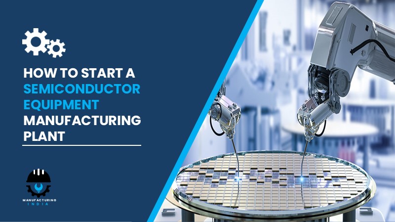
Setting up a semiconductor equipment manufacturing plant in India presents a compelling investment case at the strategic intersection of the country’s national semiconductor self-sufficiency mission, the global semiconductor industry’s extraordinary demand surge, and India’s rapidly developing precision engineering and electronics manufacturing ecosystem. Semiconductor equipment the specialised machinery and tools used in the fabrication, assembly, testing, and packaging of semiconductor devices such as integrated circuits, memory chips, and microprocessors is the foundational input that enables every semiconductor fabrication facility in the world to operate. As the global semiconductor industry accelerates investment in advanced node manufacturing to serve AI, 5G, electric vehicles, cloud computing, and IoT applications, demand for the equipment that makes chip production possible is growing at an equally accelerating pace. Global semiconductor sales reached USD 75.3 billion in November 2025, representing a 29.8% increase compared to November 2024 a surge reported by the Semiconductor Industry Association that is directly driving increased capital expenditure by chipmakers and accelerating growth in the global semiconductor equipment market.
India’s strategic transformation into a semiconductor manufacturing nation is creating an unprecedented domestic demand opportunity for semiconductor equipment producers. In February 2026, India launched Semiconductor Mission 2.0 under the Union Budget 2026, with an allocation of ₹1,000 crore for FY27, specifically emphasising the strengthening of domestic capabilities in semiconductor equipment and materials, developing full-stack Indian intellectual property, and reinforcing supply chains. This mission-level policy commitment combined with India’s established precision manufacturing clusters in Karnataka, Maharashtra, Tamil Nadu, and Uttar Pradesh, its large pool of engineering and electronics talent, and a growing network of semiconductor fabrication investments creates the demand foundation, policy support, and talent infrastructure required to build a commercially viable semiconductor equipment manufacturing plant in India today.
A semiconductor equipment manufacturing plant in India is positioned within a global market valued at USD 109.87 billion in 2025 growing at 7.2% CAGR toward USD 205.76 billion by 2034, directly supported by India’s Semiconductor Mission 2.0 launched in February 2026, global semiconductor sales surging 29.8% year-on-year in November 2025, and India’s first dedicated semiconductor equipment facility inaugurated by KASFAB Tools in January 2025. With gross profit margins of 50–60% and net margins of 20–30% among the highest across all manufacturing categories this investment delivers exceptional returns for early-mover investors in India’s most strategically critical technology manufacturing sector.
What is Semiconductor Equipment?
Semiconductor equipment refers to specialised machinery and tools used in the fabrication, assembly, testing, and packaging of semiconductor devices such as integrated circuits, memory chips, and microprocessors. These equipment systems support critical processes including wafer fabrication, lithography, etching, deposition, doping, inspection, and testing. Semiconductor equipment is designed to operate at extremely high precision and cleanliness levels to meet the stringent manufacturing requirements of nanometre-scale chip production.
Continuous innovation in equipment technology is essential to support advanced node manufacturing, improve yield, and reduce defect rates across both front-end wafer fabrication and back-end assembly and testing operations. The market includes both front-end equipment used in wafer fabrication and back-end equipment used in assembly and testing operations — covering applications in wafer fabrication and processing, semiconductor assembly and packaging, chip inspection and testing, and both advanced node and legacy node manufacturing. The primary production method involves precision component fabrication and sourcing, mechanical and electronic sub-assembly, software integration and system calibration, cleanroom testing and validation, final assembly, inspection, and packaging. End-use industries served include semiconductor manufacturing fabs, integrated device manufacturers (IDMs), foundries and OSAT companies, and the broader electronics and technology sector.
Cost of Setting Up a Semiconductor Equipment Manufacturing Plant in India
The total investment required to establish a semiconductor equipment manufacturing plant in India depends on plant capacity, product complexity and equipment type, geographic location, cleanroom specification requirements, level of automation, and compliance with precision manufacturing quality standards. Investors must account comprehensively for both one-time capital expenditure and recurring operational costs when preparing a feasibility study or detailed project report (DPR).
1. Capital Expenditure (CapEx)
Land and Site Development constitutes a substantial foundational investment. Costs for land registration, boundary construction, internal road layout, drainage infrastructure, and site levelling vary based on whether the facility is within a government-notified semiconductor or electronics manufacturing zone, a Special Economic Zone (SEZ), or on privately acquired industrial land. Electronics manufacturing clusters in Karnataka (Doddaballapur and Bengaluru), Maharashtra, Tamil Nadu, and Uttar Pradesh offer infrastructure-ready sites with proximity to engineering talent pools, precision component suppliers, and semiconductor fab buyer networks.
Civil Works and Construction encompasses the main precision machining and sub-assembly hall with vibration-damped flooring for high-precision CNC operations, a cleanroom assembly and calibration area meeting the ISO 14644 cleanliness class appropriate for the equipment type being manufactured, quality control and testing laboratory, software integration and calibration suite, finished equipment storage and packaging area, and administrative block. Cleanroom construction including HVAC systems for particulate control, gowning areas, positive pressure maintenance, and continuous environment monitoring represents a significantly higher cost per square metre than standard industrial construction and is a mandatory requirement for semiconductor equipment assembly and validation.
Machinery and Equipment represent the single largest component of capital expenditure. Key machinery required for a semiconductor equipment manufacturing plant includes:
- CNC machining and fabrication systems
- Cleanroom assembly equipment
- Precision calibration and testing systems
- Software and control integration tools
- Packaging and material handling equipment
Other Capital Costs include the effluent treatment plant (ETP), pre-operative expenses covering regulatory filings and feasibility study preparation, intellectual property licensing costs for proprietary technology elements, plant commissioning charges, cleanroom certification costs, utility connection fees, and import duties applicable to specialised CNC precision machining equipment or cleanroom-grade assembly and testing systems sourced internationally.
Request a Sample Report for In-Depth Market Insights: https://www.imarcgroup.com/semiconductor-equipment-manufacturing-plant-project-report/requestsample
2. Operational Expenditure (OpEx)
Raw Material Cost accounts for approximately 40–50% of total OpEx a moderate ratio relative to process-intensive manufacturing categories, reflecting the high value-added engineering and precision manufacturing content of finished semiconductor equipment relative to its material inputs. The primary inputs are specialised metals including stainless steel for high-purity vacuum chambers and process chambers, ceramics for dielectric and thermal components, precision motors for motion control systems, and control systems including electronic control boards, sensors, and actuators. Stainless steel used extensively in vacuum system and process chamber construction represents the largest single material cost item. Investors are advised to negotiate long-term supply contracts with qualified specialty metals distributors, precision ceramic manufacturers, and electronics control system suppliers to stabilise input costs and ensure the component quality consistency essential for semiconductor equipment performance reliability. For India-based manufacturers serving global semiconductor fabs and IDMs, the ability to source materials and sub-components at international purity and specification standards is a prerequisite for product acceptance by major customers.
Utility Costs – covering electricity for CNC machining systems, cleanroom HVAC operation, precision calibration equipment, software integration systems, and facility operations account for approximately 10–15% of total OpEx. Cleanroom HVAC systems, which must maintain continuous temperature, humidity, and particulate control for clean assembly environments, contribute a significant and continuous electricity load that must be managed through energy-efficient HVAC design and competitive industrial tariff access.
Other Operating Costs include outbound transportation and specialist logistics for large, precision-engineered equipment which requires vibration-isolated crating and climate-controlled shipping containers to semiconductor fabs, IDMs, foundries, OSAT companies, and electronics manufacturers globally; packaging materials including custom-engineered protective enclosures; employee salaries and wages for precision engineers, CNC machinists, cleanroom assembly technicians, software integration specialists, and quality validation engineers; equipment maintenance; quality assurance and customer acceptance testing; depreciation on civil and machinery assets; and applicable taxes including GST. By the fifth year of operations, total operational costs are expected to increase substantially due to inflation, market fluctuations, potential rises in specialised metal and precision component prices, and supply chain disruptions driven by global semiconductor equipment demand growth.
3. Plant Capacity
The proposed semiconductor equipment manufacturing facility is designed with an annual production capacity of 5,000 or more units, enabling significant economies of scale while maintaining operational flexibility across different equipment types from wafer inspection systems and testing rigs to deposition and etching subsystems. This capacity range supports the requirements of domestic semiconductor fab customers including fabs developed under India’s Semiconductor Mission 2.0, as well as global foundry and IDM customers seeking diversified, India-based equipment supply chain relationships. Capacity can be customised based on investor requirements, engineering talent availability, and target customer segment focus. Profitability improves substantially with higher capacity utilisation, particularly given the high gross margin profile of the product category.
4. Profit Margins and Financial Projections
The semiconductor equipment manufacturing plant demonstrates the strongest profitability profile across all manufacturing investment categories reviewed in this series. Gross profit margins typically range between 50–60%, reflecting the extraordinary value added through precision engineering, intellectual property integration, software content, and the application-critical performance specifications that semiconductor equipment must consistently deliver. Net profit margins range between 20–30%, making this one of the highest net margin manufacturing investments available in India’s technology manufacturing sector. A comprehensive financial analysis should include income projections, expenditure forecasts, gross and net margin tracking across Years 1 through 5, net present value (NPV), internal rate of return (IRR), payback period, and a full profit and loss account. Sensitivity analysis covering semiconductor industry capital expenditure cycle dynamics which directly determine customer equipment order volumes is particularly important for investment-grade planning in this sector.
Why Set Up a Semiconductor Equipment Manufacturing Plant in India?
India’s Semiconductor Mission 2.0 Creating Direct Policy Demand for Domestic Equipment. In February 2026, India launched Semiconductor Mission 2.0 under the Union Budget 2026 with ₹1,000 crore allocated for FY27, explicitly emphasising the strengthening of domestic capabilities in semiconductor equipment and materials, developing full-stack Indian intellectual property, and reinforcing supply chains through industry-led research initiatives and training centres. This dedicated policy and financial commitment to domestic semiconductor equipment development represents a direct demand creation mechanism for new Indian equipment manufacturers a policy environment without precedent in India’s electronics manufacturing history.
Surging Global Semiconductor Sales Driving Equipment Capital Expenditure. Global semiconductor sales reached USD 75.3 billion in November 2025, representing a 29.8% increase compared to the November 2024 total of USD 58.0 billion and 3.5% more than the October 2025 total of USD 72.7 billion, as reported by the Semiconductor Industry Association. This exceptional sales performance directly drives increased capital expenditure by chipmakers on manufacturing, inspection, and testing equipment creating the investment pipeline that translates into equipment order volumes for manufacturers serving semiconductor fabs globally.
AI, 5G, and EV Applications Sustaining Multi-Year Demand Growth. Rapid adoption of artificial intelligence, high-performance computing, and 5G technologies is accelerating investment in advanced chip manufacturing across both leading-edge and mature node fabrication. The transition to smaller process nodes and advanced packaging technologies is increasing the need for sophisticated fabrication and testing equipment across the entire semiconductor production flow from wafer processing through final device testing ensuring that demand for semiconductor equipment grows in parallel with the broader semiconductor demand cycle driven by AI infrastructure buildout and EV electronics proliferation.
India’s First Dedicated Semiconductor Equipment Facility Validating Commercial Viability. In January 2025, KASFAB Tools Pvt. Ltd. launched India’s first dedicated manufacturing and assembly facility for semiconductor equipment serving global customers. The state-of-the-art facility, located in Doddaballapur, was inaugurated in the presence of global supply chain partners and customers from Fortune 100 companies — directly validating that India-based semiconductor equipment manufacturing can meet the specification and quality requirements of the world’s most demanding semiconductor industry customers, and establishing a commercial precedent that de-risks the market entry assessment for subsequent investors.
Government Support and Supply Chain Localisation Creating Structural Demand. National semiconductor initiatives and incentives globally including India’s Semiconductor Mission, US CHIPS Act, and European Chips Act are encouraging domestic semiconductor manufacturing and equipment demand through capital subsidies for fab construction and explicit localisation preferences for domestic equipment supply. India-based equipment manufacturers who qualify for domestic preference in government-supported fab procurement programmes benefit from a structural commercial advantage in the emerging Indian semiconductor supply chain.
High Entry Barriers Creating Durable Competitive Moats. Semiconductor equipment manufacturing involves advanced engineering, intellectual property, precision manufacturing capabilities, and deep customer qualification relationships creating high entry barriers that protect established players’ margins and limit competitive disruption once market position is established. For investors who successfully build qualifying engineering capabilities and customer acceptance at major fabs, this competitive moat translates into durable pricing power, long-term service revenue from installed equipment bases, and the gross margins of 50–60% that reflect this structural competitive advantage.
Manufacturing Process – Step by Step
The semiconductor equipment manufacturing process uses precision component fabrication and sourcing, mechanical and electronic sub-assembly, software integration and system calibration, cleanroom testing and validation, final assembly, inspection, and packaging as the primary production method. Below are the main stages involved in the semiconductor equipment manufacturing process flow:
- Design and Engineering: Mechanical, electrical, and software engineering teams develop equipment designs using CAD, simulation, and modelling tools, producing detailed manufacturing specifications, bill of materials, and software architecture documentation for each equipment system.
- Precision Component Fabrication – CNC Machining: CNC machining and fabrication systems produce high-precision metal components including vacuum chamber bodies, process chamber housings, robotic arm structures, and motion stage assemblies from specialised stainless steel and aluminium alloy stock, achieving the dimensional tolerances of microns required for semiconductor process equipment performance.
- Ceramic and Specialty Component Procurement: Ceramic components including dielectric rings, electrostatic chuck assemblies, and thermal management components and precision motors, actuators, sensors, and control system boards are sourced from qualified specialty suppliers against detailed specification requirements and incoming quality inspection.
- Mechanical Sub-Assembly: Cleanroom assembly equipment facilitates the assembly of fabricated and procured mechanical components into functional sub-assemblies including chamber assemblies, vacuum system modules, robotic transfer systems, and motion control stages in controlled environments that prevent particulate contamination of critical internal surfaces.
- Electronic and Control System Integration: Software and control integration tools are used to integrate electronic control boards, sensor arrays, actuators, and power supply units into the equipment’s electrical and control architecture, with wiring, connector assembly, and signal integrity verification completed to specification.
- Software Integration and Programming: Equipment control software is loaded, configured, and integrated with hardware control systems, with process recipe libraries, user interface validation, and communication protocol testing completed for compatibility with the customer’s fab automation and manufacturing execution systems.
- System Calibration: Precision calibration and testing systems calibrate all measurement, positioning, and process control parameters of the assembled equipment system against the acceptance specifications that ensure process performance at the semiconductor fab including dimensional accuracy, positional repeatability, sensor response linearity, and process uniformity.
- Cleanroom Testing and Validation: The fully assembled and calibrated equipment system is subjected to functional testing, performance qualification, and quality validation in the cleanroom environment, covering all process and mechanical parameters against the customer’s acceptance test protocol.
- Quality Inspection and Acceptance Testing: Quality assurance instruments verify that all equipment performance parameters including yield-relevant process uniformity, defect density contribution, mean time between failures (MTBF), and software functionality meet the specification acceptance criteria required for customer site delivery and commissioning.
- Packaging and Dispatch: Finished semiconductor equipment is packaged in custom-engineered protective enclosures designed to withstand the mechanical stress, vibration, and environmental conditions of long-distance shipping, and dispatched to semiconductor fabs, IDMs, foundries, OSAT companies, and electronics manufacturers via specialist semiconductor equipment logistics providers.
Key Applications
Semiconductor equipment produced at this type of facility serves four primary end-use customer and application categories within the global semiconductor manufacturing ecosystem:
- Semiconductor Foundries: Advanced semiconductor equipment for high-volume manufacturing of logic and memory chips across multiple technology nodes, serving foundry customers including leading-edge fab operators and capacity-expansion projects supported by national semiconductor missions.
- Integrated Device Manufacturers (IDMs): Equipment for in-house chip production supporting consumer electronics, automotive, and industrial semiconductor applications including front-end wafer fabrication and back-end assembly and test equipment for IDMs managing their complete chip manufacturing value chain.
- OSAT Companies: Back-end equipment for packaging, testing, and quality assurance of semiconductor devices including die-attach systems, wire bonders, encapsulation equipment, and automated test systems used by outsourced semiconductor assembly and test companies serving global chip supply chains.
- Electronics and Technology Sector: Equipment supporting chip production for smartphones, servers, networking hardware, and consumer electronics, covering both advanced node manufacturing for leading-edge applications and legacy node production for high-volume consumer and industrial devices.
Leading Semiconductor Equipment Manufacturers
The global semiconductor equipment industry is served by a small number of exceptionally well-capitalised global leaders with deep technology portfolios and long-standing fab customer relationships. Key players include:
- ASML Holding NV
- Applied Materials Inc.
- Lam Research Corp.
- Tokyo Electron Ltd.
- KLA Corp.
Timeline to Start the Plant
Investors planning to establish a semiconductor equipment manufacturing plant in India should anticipate the following project development phases, with an overall timeline typically ranging from 24 to 36 months given the cleanroom construction and equipment qualification requirements:
- Feasibility study and project report preparation
- Land acquisition and site development
- Regulatory approvals and environmental clearances
- Factory licence and fire safety compliance
- Machinery procurement and installation
- Raw material supplier agreements and supply chain setup
- Trial production and quality testing
- Commercial production launch
Licences and Regulatory Requirements
Starting a semiconductor equipment manufacturing unit in India requires several approvals:
- Business registration (Proprietorship, LLP, or Private Limited Company)
- Factory Licence under the Factories Act
- Environmental Clearance from the State Pollution Control Board
- GST Registration
- Fire Safety NOC
- Effluent Treatment Plant (ETP) operational clearance for chemical and process waste management
- Occupational Health and Safety compliance covering CNC machine operation, cleanroom chemical handling, and high-voltage electrical system testing
- Semiconductor Mission 2.0 registration for eligibility to access domestic equipment development incentives and government-supported fab procurement preferences
- Export certification and customs compliance for semiconductor equipment exported to international fab and IDM customers
- Intellectual property protection registration for proprietary equipment designs, software, and process patents developed in India
Key Challenges to Consider
Extreme Precision Engineering and Cleanroom Standards. Semiconductor equipment must consistently deliver nanometre-scale process accuracy across thousands of operational hours in customer fab environments. Achieving and maintaining the precision manufacturing standards required including cleanroom assembly protocols, sub-micron dimensional tolerances, and particle contamination control — demands significant infrastructure investment, rigorous quality management systems, and highly trained engineering personnel throughout the production process.
Deep Technology and Intellectual Property Requirements. Semiconductor equipment involves advanced engineering knowledge, proprietary process algorithms, and specialised software that represent multi-year development investments and significant intellectual property assets. New entrants must invest substantially in R&D capability, technology licensing, or industry partnerships to build a product portfolio capable of meeting the performance specifications required for acceptance at global semiconductor fabs and IDMs.
Semiconductor Industry Capital Expenditure Cyclicality. The semiconductor equipment market is subject to pronounced cycles of capital expenditure expansion and contraction driven by semiconductor demand cycles, memory pricing dynamics, and fab capacity management decisions by major chipmakers. Understanding and managing through the inherent demand cyclicality of this market requires careful working capital management, flexible production capacity, and diversification across multiple equipment types and customer segments.
Customer Qualification Lead Times. Gaining approval to supply semiconductor equipment to a major fab or IDM requires an extensive technical qualification process including process performance testing, reliability qualification, and integration testing with the customer’s fab automation systems that can take 12 to 24 months or longer before commercial revenue begins. This extended qualification cycle requires investors to plan for a prolonged pre-revenue investment phase and to fund the technical qualification process as a mandatory customer acquisition cost.
Competition from Established Global Technology Leaders. The global semiconductor equipment market is dominated by ASML, Applied Materials, Lam Research, Tokyo Electron, and KLA companies with decades of technology development, billions in R&D investment, and deeply embedded customer relationships at every major semiconductor fab globally. New Indian market entrants must focus on specific equipment categories, subsystem manufacturing, or localisation-driven demand created by India’s Semiconductor Mission 2.0 to build sustainable competitive positioning.
Skilled Engineering Workforce for Precision Semiconductor Equipment Manufacturing. Operating CNC precision machining systems, cleanroom assembly equipment, and precision calibration and testing systems requires engineers with specialised training in precision mechanical engineering, vacuum technology, semiconductor process physics, control systems, and equipment qualification protocols. Sourcing and retaining this specialised talent pool which is in global-scale competition across every semiconductor ecosystem is the most critical and persistently challenging human capital requirement for this manufacturing category.
Frequently Asked Questions
1. How much does it cost to set up a semiconductor equipment manufacturing plant in India?
The total cost depends on plant capacity (5,000+ units per annum), equipment type portfolio, cleanroom specification, and location. CapEx covers land, cleanroom-standard civil construction, and machinery including CNC machining and fabrication systems, cleanroom assembly equipment, precision calibration and testing systems, software and control integration tools, and packaging and material handling equipment, along with pre-operative, IP licensing, and regulatory costs.
2. Is semiconductor equipment manufacturing profitable in India in 2026?
Yes with gross margins of 50–60% and net margins of 20–30%, this is the highest-margin manufacturing investment category reviewed in this series. Supported by global semiconductor sales surging 29.8% year-on-year in November 2025, India’s Semiconductor Mission 2.0 launched in February 2026, and a global market growing at 7.2% CAGR toward USD 205.76 billion by 2034, the investment presents an exceptional profitability case for investors who can build the required engineering capabilities.
3. What machinery is required for a semiconductor equipment manufacturing plant in India?
Key equipment includes CNC machining and fabrication systems, cleanroom assembly equipment, precision calibration and testing systems, software and control integration tools, and packaging and material handling equipment.
4. What licences and approvals are required to start a semiconductor equipment manufacturing plant in India?
Required approvals include business registration, Factory Licence, Environmental Clearance, GST Registration, Fire Safety NOC, ETP operational clearance, Occupational Health and Safety compliance, Semiconductor Mission 2.0 registration, export certification for international customers, and IP protection registration for proprietary equipment designs.
5. What raw materials are needed for semiconductor equipment manufacturing?
The primary raw materials are specialised metals including stainless steel, ceramics, precision motors, and control systems. Additional inputs include aluminium alloys, vacuum-grade seals and gaskets, electronic control boards, sensors, actuators, high-purity process materials, and specialty cleaning agents for cleanroom-standard component processing.
6. What are the environmental compliance requirements for a semiconductor equipment manufacturing plant in India?
Environmental Clearance from the State Pollution Control Board is required, along with ETP operational clearance for managing chemical and process waste streams from CNC machining coolants, cleanroom chemical cleaning agents, and calibration materials. Compliance with solid waste management rules for metal machining swarf and chemical waste disposal is mandatory.
7. What is the best location to set up a semiconductor equipment manufacturing plant in India?
States with established precision engineering and electronics manufacturing ecosystems, engineering talent pools, and proximity to India’s emerging semiconductor fab investments — including Karnataka (Bengaluru and Doddaballapur), Maharashtra, Tamil Nadu, and Uttar Pradesh — offer the best combination of skilled workforce availability, precision component supply chain access, customer proximity, and policy incentive support under Semiconductor Mission 2.0.
8. What is the break-even period for this type of plant in India?
The break-even period depends on equipment type focus, customer qualification timelines, order volume ramp, and the extended pre-revenue technical qualification phase required before commercial fab customers accept new equipment suppliers. A full NPV and IRR analysis incorporating the qualification phase investment and sensitivity testing for semiconductor capex cycle dynamics is essential for investment-grade financial planning.
9. What government incentives are available for semiconductor equipment manufacturers in India?
India’s Semiconductor Mission 2.0, launched in February 2026 with ₹1,000 crore for FY27, provides direct support for domestic semiconductor equipment development, IP creation, and supply chain strengthening. Design-linked incentives, electronics manufacturing PLI scheme benefits, state-level industrial incentives in Karnataka and Maharashtra, Semiconductor Mission equipment procurement preferences for India-based suppliers, and export promotion support through electronics export councils all provide relevant financial and market access support for qualifying semiconductor equipment manufacturing investments.
Key Takeaways for Investors
A semiconductor equipment manufacturing plant in India represents the highest-margin and most strategically significant manufacturing investment opportunity available in India’s technology sector today positioned within a global market valued at USD 109.87 billion in 2025 growing at 7.2% CAGR toward USD 205.76 billion by 2034, directly supported by India’s Semiconductor Mission 2.0 with ₹1,000 crore in FY27 allocation, and validated by KASFAB Tools’ January 2025 inauguration of India’s first dedicated semiconductor equipment facility at Doddaballapur serving Fortune 100 semiconductor customers. Financial viability is demonstrated at a production capacity of 5,000 or more units per annum, with gross margins of 50–60% and net margins of 20–30% the strongest profitability profile across all manufacturing categories in this investment series. With global semiconductor sales surging 29.8% year-on-year in November 2025 and AI, 5G, electric vehicle, and advanced node chip demand all sustaining extraordinary capital expenditure cycles among the world’s leading chipmakers, long-term demand sustainability and commercial opportunity for India-based semiconductor equipment manufacturers are both exceptionally large and structurally durable for the decade ahead.