
Key takeaways
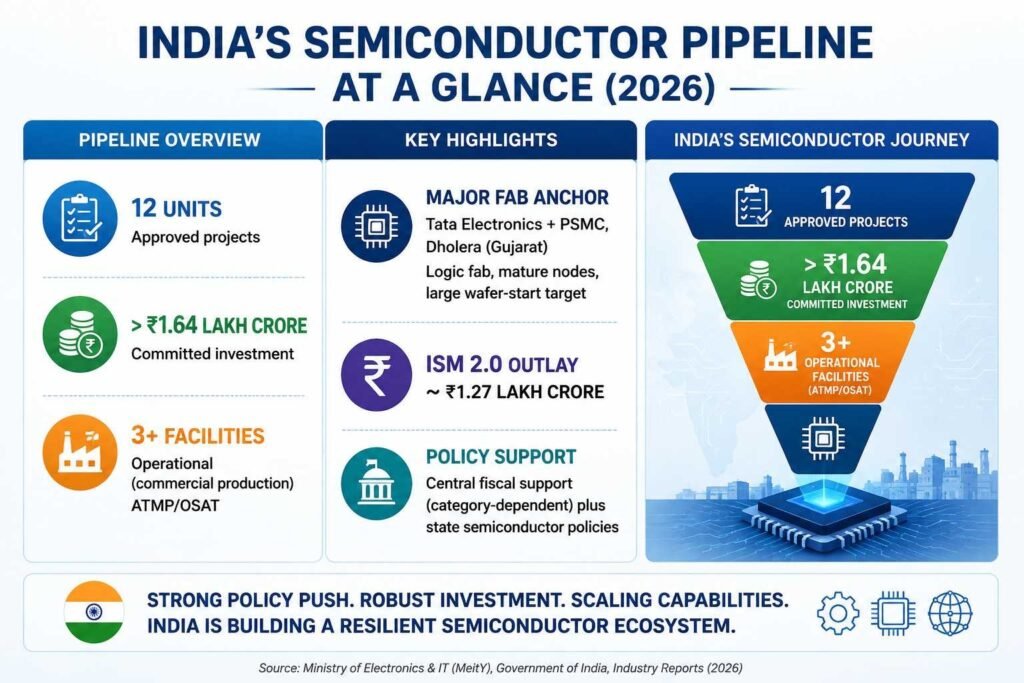
- India has moved from policy intent to execution: under the India Semiconductor Mission, 12 manufacturing projects have been approved with cumulative committed investment exceeding ₹1.64 lakh crore, and multiple ATMP/OSAT units are already in commercial production.
- Semicon / ISM 2.0, with an outlay of about ₹1.27 lakh crore, extends support across design, equipment, materials, additional fabs and advanced packaging, raising the bar for projects that are not only approved but operable.
- Facility type (silicon fab, compound semiconductor, OSAT/ATMP, display) drives capital intensity, utility demand, cleanroom specification and timeline. Planning errors at this stage are expensive to reverse.
- Site selection, ultra-reliable power, ultra-pure water, vibration control, cleanroom design and statutory sequencing often determine whether a plant ramps on schedule or stalls after equipment arrives.
- Technology partnerships and incentives matter, but disciplined facility planning is what converts approved projects into yield, certification and sustained output.
Introduction
India’s semiconductor push is no longer only a headline about incentives. Approved projects span packaging, compound semiconductors and a major logic fab. Several assembly and test facilities in Gujarat are already shipping products, while larger fabrication investments are moving through construction and tool-install phases. Policy continuity under ISM 2.0 signals that more capacity will be sought over the coming years.
For sponsors, the competitive question is shifting. Winning an approval is necessary. Building a facility that can qualify tools, hit yield targets and stay online is what decides commercial success. That outcome depends heavily on facility planning: model selection, site and utilities, cleanroom and tool hook-up design, and a construction–commissioning sequence that respects semiconductor realities rather than generic industrial practice.
The Scale of the Race in 2026
Under ISM 1.0, the government has approved 12 semiconductor manufacturing units with investment commitments above ₹1.64 lakh crore. The mix includes one silicon fabrication plant, compound semiconductor and display-related capacity, and a majority of ATMP/OSAT packaging units. Three facilities (including major ATMP/OSAT operations in Sanand) have entered commercial production, with further units expected to come online through 2026 and beyond. The first major silicon fab is progressing toward commissioning later in the decade, making facility execution and qualification readiness increasingly important.
ISM 2.0 adds a large fiscal outlay and a broader ecosystem focus (design, equipment, materials, more fabs and advanced packaging). Public statements also point to additional plants over a multi-year horizon. The pipeline is real. So is the execution risk for any project that under-plans the physical plant.
Facility Model Choice Sets Every Downstream Constraint
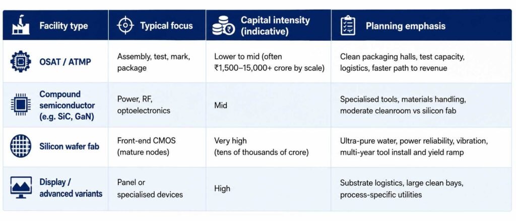
Choosing OSAT for speed-to-market versus a fab for strategic depth is a business decision. Once chosen, cleanroom class, utility capacity, structural vibration limits and construction sequence must follow that choice. Retrofitting an under-specified shell or utility plant after tools are ordered is one of the costliest failures in this sector.
Consult IMARC Engineering for Semiconductor Facility Planning: https://www.imarcengineering.com/contact-us
Where Facility Planning Decides Success
Site and environment: Clusters in Gujarat (Sanand, Dholera), Assam (Jagiroad), and emerging locations in other states offer policy and ecosystem advantages. Beyond incentives, planners must validate seismic and vibration conditions for lithography and precision tools, air quality impact on cleanroom load, water availability for ultra-pure systems, and 24×7 power quality. Weak site due diligence shows up later as tool instability or utility shortfalls.
Utilities and cleanroom: Semiconductor facilities depend on continuous, high-quality power, large volumes of ultra-pure water, specialised gases and tightly controlled HVAC. Cleanroom design must match process ISO classes, pressure cascades and contamination control. Utility plants sized for average load rather than peak and redundancy requirements become bottlenecks during ramp.
Construction and tool sequence: Shell, cleanroom fit-out, utility hook-up and tool move-in must be sequenced so that large tools can be installed before irreversible closures and so that commissioning does not wait on incomplete services. Generic construction programmes that ignore tool-install logic create avoidable delay.
Regulatory and licensing path: Environmental clearance, factory and fire approvals, hazardous material and gas handling permissions, and any sector-specific conditions must sit on the same master schedule as civil and cleanroom works. Facility drawings and EMP commitments should stay consistent with the design that will actually be built.
Workforce and operations readiness: Cleanroom discipline, tool qualification and yield learning curves require trained technicians and engineers. Facility planning that ignores training space, gowning flow and early hiring timelines slows the path from mechanical completion to qualified output.
How IMARC Engineering Supports Semiconductor Facility Planning and Project Readiness
IMARC Engineering assists investors and project teams planning semiconductor and advanced electronics manufacturing facilities in India with engineering-led feasibility and project definition. Support includes:
- Facility model assessment (OSAT/ATMP, compound semiconductor, wafer fab pathways) against capital, timeline and market strategy.
- Site evaluation covering utilities, vibration and environmental constraints relevant to precision manufacturing.
- Cleanroom, utility and layout concept planning aligned to process and contamination-control needs.
- Capex framing, schedule logic and risk identification for construction through tool-install and qualification.
- Regulatory pathway mapping for environmental, factory and related approvals.
- Integration of facility planning with broader project documentation used for investment and incentive processes.
The focus is on reducing the gap between approved intent and an operable plant, so that technology partnerships and incentives are matched by a facility that can actually run.
For a full setup roadmap covering technology, infrastructure, cost and approvals, see the complete guide on How to Set Up a Semiconductor Manufacturing Facility in India: https://www.imarcengineering.com/blog/how-to-set-up-a-semiconductor-manufacturing-facility-in-india
Final thoughts
India’s semiconductor manufacturing race will be won by projects that treat the factory as a precision system, not only as a subsidised building. Policy has created a real pipeline and a second wave of support under ISM 2.0. Facility planning (model choice, site, utilities, cleanroom, sequence and compliance) is what turns that pipeline into stable production. Sponsors who invest in that discipline early improve their odds of joining the list of plants that ship, not only the list of plants that were announced.
Contact Us:
IMARC Engineering
Phone: +91-120-433-0800
Email: sales@imarcengineering.com
India: C-130, Sector 2, Noida, Uttar Pradesh 201301
LinkedIn: https://www.linkedin.com/showcase/imarc-engineering/
About the Author