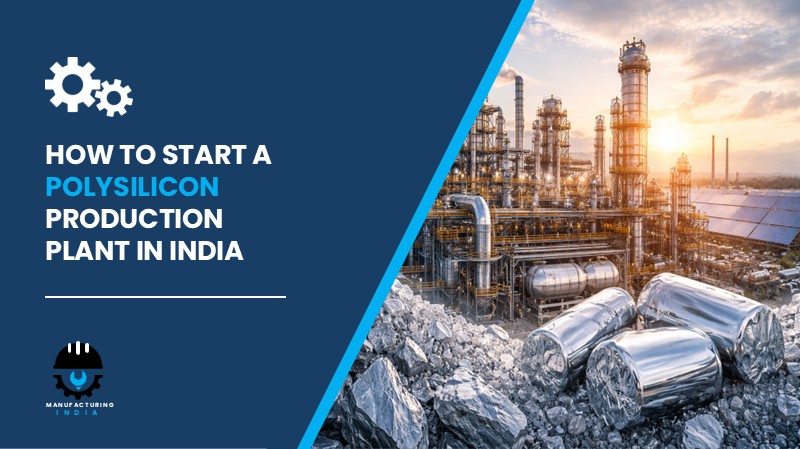
Setting up a polysilicon production plant in India presents a compelling investment case at a time when the country’s solar energy ambitions, semiconductor manufacturing aspirations, and strategic supply chain self-reliance imperatives are converging around a single critical material that India currently imports almost entirely. Polysilicon — or polycrystalline silicon — is the highly purified form of silicon that serves as the core raw material for solar photovoltaic cells and semiconductor devices, and it sits at the absolute foundation of two of the most strategically important industrial transitions of the 21st century: the global clean energy revolution and the digitalisation of the world economy. Without domestic polysilicon production, India’s solar panel manufacturing ambitions and semiconductor fabrication aspirations rest on a foreign supply chain that is currently concentrated, geopolitically sensitive, and subject to disruptions that can cascade across the country’s entire renewable energy deployment programme.
India’s structural case for polysilicon production is compelling and policy-supported at the highest levels. The government’s PM Surya Ghar Muft Bijli Yojana rooftop solar initiative enables residential households to receive up to 300 units of free electricity per month, with eligible families provided direct financial subsidies of up to INR 78,000 for rooftop solar installation — a programme that is driving mass solar adoption and creating sustained, government-funded demand for the entire solar manufacturing value chain from polysilicon through wafers, cells, and modules. India’s 500 GW renewable energy target by 2030 requires a scale of domestic solar PV manufacturing that cannot be sustained without domestic polysilicon supply. The PLI scheme for solar PV manufacturing and the semiconductor mission together create a policy architecture that makes establishing polysilicon production in India not merely commercially attractive but nationally strategic — directly addressing the supply chain vulnerability that stands between India and its clean energy and technology self-sufficiency ambitions.
Investing in a polysilicon production plant in India today aligns India’s 500 GW renewable energy target, the PM Surya Ghar rooftop solar programme, and the government’s semiconductor mission with a global polysilicon market growing from USD 12.91 Billion in 2025 to USD 26.46 Billion by 2034 at an 8.3% CAGR. With gross profit margins of 35–45% and net profit margins of 20–30%, the unit economics are strong, and the facility’s energy-intensive but technically scalable production model — designed for 5,000 to 20,000 MT annually — supports commercially sound and strategically vital returns across a long-term investment horizon.
What is Polysilicon?
Polysilicon, or polycrystalline silicon, is a highly purified form of silicon that serves as the core raw material in the manufacturing of solar photovoltaic cells and semiconductor devices. The production process starts with metallurgical-grade silicon, which operators refine through chemical processes — including the Siemens method — to create ultra-high purity material suitable for electronic and photovoltaic applications. Polysilicon typically exists as solid rods or granular chunks, which workers melt down to create ingots and wafers through a process of recrystallisation. The wafers serve as the fundamental component for solar panels, integrated circuits, and various microelectronic components.
Polysilicon provides dependable performance because it combines outstanding electrical conductivity with thermal stability and controlled impurity levels. The purity required differs by application: solar-grade polysilicon typically requires 99.9999% (6N) purity, while semiconductor-grade polysilicon demands 99.999999999% (11N) purity or higher. These purity levels are achieved through the Siemens process of chemical vapour deposition (CVD) or the fluidised bed reactor (FBR) method. Polysilicon maintains its status as a vital material for global clean energy and technology supply chains because it serves essential functions in both renewable energy production and advanced electronics manufacturing.
The primary production process covers metallurgical-grade silicon purification, trichlorosilane synthesis, chemical vapour deposition (CVD) via the Siemens process or fluidised bed reactor (FBR) method, hydrogen recovery, by-product recycling, rod harvesting or granulation, quality inspection, and packaging. End-use industries served include solar photovoltaic manufacturing, semiconductor fabrication, electronics, and integrated circuit industries. Applications span solar wafers, photovoltaic cells, microchips, power electronics, and electronic-grade silicon components.
Cost of Setting Up a Polysilicon Production Plant in India
The cost of establishing a polysilicon production plant in India depends on production capacity, technology selection between the Siemens CVD process and the fluidised bed reactor method, target product grade between solar-grade and semiconductor-grade polysilicon, geographic location — particularly the availability and cost of reliable high-capacity electricity — and the stringent chemical safety and purity compliance requirements applicable to polysilicon supplied to solar and semiconductor manufacturers.
1. Capital Expenditure (CapEx)
Land and Site Development forms a foundational component of total capital investment, covering land acquisition charges, site registration, boundary development, chemical containment and drainage infrastructure, and site utilities — most critically, connection to high-capacity electricity supply, which is the dominant operational cost driver for this energy-intensive process. Investors may explore industrial estates in states with competitive industrial electricity tariffs, proximity to silicon mining or metallurgical silicon production — Himachal Pradesh, Jammu and Kashmir, Chhattisgarh, and Gujarat are relevant — and logistics connectivity to solar panel manufacturing clusters in Rajasthan, Gujarat, and Tamil Nadu that constitute the primary domestic customer base for solar-grade polysilicon.
Civil Works and Construction cover the main production building housing CVD reactor halls or FBR systems — which require specialised high-temperature, high-pressure, and corrosion-resistant construction standards — distillation column skids, hydrogen recovery and recycling infrastructure, by-product processing facilities, trichlorosilane storage, quality control laboratory, rod harvesting or granulation areas, finished goods warehousing, and an administrative block. The scale and technical complexity of reactor hall construction, high-pressure vessel support structures, and hydrogen safety infrastructure significantly exceed conventional chemical plant civil requirements.
Machinery and Equipment represent the largest single component of total CapEx for a polysilicon production plant. Key machinery required includes:
- CVD reactors
- Distillation columns
- Hydrogen recovery systems
- Gas compressors
- Filtration systems
- Packaging units
Other Capital Costs include an effluent treatment plant (ETP) for managing silicon tetrachloride and other by-product waste streams, hydrogen safety infrastructure including leak detection, explosion-proof electrical systems and ventilation, trichlorosilane storage safety systems, pre-operative expenses, environmental clearance costs, commissioning and trial run charges, and import duties on specialised CVD reactor systems or distillation columns not available domestically at the required specification.
Request a Sample Report for In-Depth Market Insights: https://www.imarcgroup.com/polysilicon-production-cost-analysis-report/requestsample
2. Operational Expenditure (OpEx)
Raw Material Cost is the dominant operational expense, accounting for approximately 50–60% of total OpEx. The primary raw materials are metallurgical silicon, hydrochloric acid, and hydrogen. Metallurgical silicon — produced from quartz quartzite through carbothermal reduction in electric arc furnaces — is the silicon feedstock that enters the polysilicon purification process. It is produced in India and available domestically, providing a raw material localisation advantage. Hydrochloric acid is used in trichlorosilane synthesis, and hydrogen is consumed both as a reactant in CVD deposition and recovered and recycled from reactor off-gas through hydrogen recovery systems. Long-term procurement contracts with reliable metallurgical silicon suppliers and industrial gas providers are essential for cost stability.
Utility Cost is the second-largest OpEx component, representing 30–40% of total operating expenses — an unusually high utility proportion that reflects the extreme energy intensity of the CVD Siemens process. Electricity consumption for reactor heating, distillation column operation, gas compression, and hydrogen recovery constitutes the dominant utility cost. This is the most critical site selection parameter for any polysilicon production investment: securing access to competitively priced, reliable industrial electricity supply is as strategically important as raw material procurement. Continual technological advancements in the Siemens process and fluidised bed reactor methods are improving production efficiency and reducing energy consumption, progressively improving the OpEx profile of newer production installations.
Other Operating Costs include transportation and distribution to solar wafer manufacturers, semiconductor fabrication facilities, and electronics producers, specialised packaging for high-purity polysilicon in inert atmosphere containers, salaries and wages for chemical engineers and quality control specialists, routine machinery maintenance including reactor electrode replacement and distillation column servicing, hydrogen recovery system upkeep, depreciation on high-value capital equipment, and applicable taxes. By the fifth year of operations, total operational costs are projected to increase substantially due to inflation, electricity tariff changes, metallurgical silicon price movements, supply chain disruptions, and shifts in the global polysilicon and clean energy economy.
3. Plant Capacity
The proposed production facility for polysilicon is designed with an annual production capacity ranging between 5,000 and 20,000 metric tonnes, enabling economies of scale while maintaining operational flexibility across the solar-grade and semiconductor-grade product mix. Plant capacity can be customised per investor requirements and phased in line with secured off-take agreements with domestic solar manufacturers or semiconductor fabrication facilities. Profitability improves with higher capacity utilisation, with energy cost per tonne declining significantly at higher throughput rates — making capacity utilisation discipline and secured customer volumes the most important determinants of financial performance in polysilicon production.
4. Profit Margins and Financial Projections
The financial projections for a polysilicon production plant demonstrate strong profitability potential under normal operating conditions. Gross profit margins typically range between 35–45%, supported by stable and growing demand from the solar PV manufacturing and semiconductor industries. Net profit margins are projected at 20–30%. A comprehensive financial analysis covering NPV (net present value), IRR (internal rate of return), payback period, gross margin progression, and net margin development across a five-year horizon is essential before committing capital. The project’s ROI profile and long-term sustainability are assessed against realistic assumptions on capital investment, production capacity utilisation, metallurgical silicon and electricity pricing trends, and demand outlook from the solar photovoltaic manufacturing and semiconductor fabrication end-use sectors.
Why Set Up a Polysilicon Production Plant in India?
Expanding Solar Installations and India’s 500 GW Renewable Energy Target. Global renewable energy targets drive continuous demand for polysilicon, and India’s own targets are among the world’s most ambitious. With the government’s PM Surya Ghar Muft Bijli Yojana rooftop solar programme providing subsidies of up to INR 78,000 per eligible household and enabling up to 300 units of free electricity monthly, the domestic pull for solar installations is being directly stimulated by government fiscal commitment. Every gigawatt of solar capacity requires polysilicon at the base of the manufacturing chain, and India’s trajectory toward 500 GW by 2030 creates a domestic demand obligation that can only be sustainably met through domestic polysilicon production.
Strategic Semiconductor Material and National Supply Chain Security. Polysilicon is an essential input for electronics and microchip manufacturing beyond its solar applications. As India’s semiconductor mission seeks to establish domestic chip fabrication capability, domestic polysilicon production becomes a supply chain security imperative — allowing India to control a critical node in the electronics manufacturing value chain rather than remaining dependent on concentrated global suppliers. Government policy incentives for domestic solar and semiconductor production directly boost investment attractiveness for upstream polysilicon capacity.
Record Global Solar PV Capacity Additions Sustaining Demand. The polysilicon market is experiencing sustained growth amid record additions to solar PV capacity worldwide. Governments are accelerating clean energy transitions, driving large-scale investments in utility-scale solar projects and rooftop installations that sustain high polysilicon consumption volumes. In February 2026, United Solar Holding began polysilicon manufacturing operations at its Sohar Freezone facility — the largest solar manufacturing plant in the Middle East — with USD 900 Million in funding enabling 40 gigawatts of annual solar module production while enhancing local photovoltaic supply chain networks. This scale of new solar manufacturing capacity directly increases global polysilicon demand.
High Entry Barriers Supporting Margin Stability. Advanced purification technology — particularly the Siemens CVD process and fluidised bed reactor methods — limits competition in polysilicon production to technically capable, heavily capitalised producers who have mastered the energy-intensive, chemically complex process. These technical barriers favour established producers with strong engineering capability and process control expertise, creating a defensible competitive moat once production scale and quality certification are achieved.
Technological Advancements Improving Production Economics. Continual technological advancements in the Siemens process and fluidised bed reactor methods are improving production efficiency and reducing energy consumption per unit of polysilicon produced — the most critical cost driver in the economics of this production. As India establishes new production capacity using state-of-the-art reactor technology, it can benefit from these efficiency improvements from the first day of operation rather than carrying the cost burden of older, less efficient legacy installations.
Global Supply Chain Diversification Opportunity. As supply chains diversify and countries prioritise domestic manufacturing capacity, polysilicon production continues to attract strategic investments globally. In December 2025, China established Beijing Guanghe Qiancheng Technology Co. through a CNY 3 Billion polysilicon consolidation platform, where major producers operate to control industry overcapacity through acquisitions and plant closures. This consolidation initiative is expected to affect polysilicon pricing while introducing new pricing methods that will determine future capacity growth in the photovoltaic industry — a development that makes diversified non-Chinese polysilicon supply capacity more strategically valuable to solar manufacturers globally, including Indian producers.
Production Process — Step by Step
The polysilicon production process uses metallurgical-grade silicon purification, trichlorosilane synthesis, chemical vapour deposition (CVD) via the Siemens process or fluidised bed reactor (FBR) method, hydrogen recovery, by-product recycling, rod harvesting or granulation, quality inspection, and packaging as the primary production method. Each stage requires precisely controlled temperature, pressure, gas composition, and flow parameters to achieve the ultra-high purity levels required for solar and semiconductor applications.
- Metallurgical Silicon Receipt and Preparation: Metallurgical-grade silicon — containing approximately 98–99% silicon — is received from suppliers, inspected for grade and composition, and crushed to the particle size required for efficient trichlorosilane synthesis.
- Trichlorosilane Synthesis: Prepared metallurgical silicon is reacted with hydrochloric acid in fluidised bed reactors at elevated temperature and pressure to produce trichlorosilane (HSiCl₃) — the intermediate silicon compound that is subsequently purified and used as the silicon feedstock for CVD polysilicon deposition.
- Trichlorosilane Purification by Distillation: The trichlorosilane-containing reaction product stream is processed through distillation columns to separate and purify trichlorosilane from silicon tetrachloride, unreacted hydrochloric acid, and trace metal chloride impurities, achieving the purity level required for high-quality polysilicon deposition.
- Chemical Vapour Deposition (CVD) — Siemens Process: Purified trichlorosilane and hydrogen are fed into CVD reactors — Siemens-type bell-jar reactors — where they undergo thermal decomposition and hydrogen reduction at the surface of heated silicon seed rods at 1,050–1,150°C. Silicon deposits onto the seed rods, building them up into thick polysilicon rods over extended deposition cycles.
- Hydrogen Recovery: Off-gas from CVD reactors — containing unreacted hydrogen, trichlorosilane, hydrogen chloride, and silicon tetrachloride — is processed through hydrogen recovery systems to separate and recycle hydrogen back to the CVD process, reducing both utility cost and environmental emissions.
- By-product Recycling: Silicon tetrachloride by-product is hydrogenated back to trichlorosilane through a hydrogenation step, closing the silicon material loop and reducing raw material consumption per tonne of polysilicon produced.
- Rod Harvesting or Granulation: At the end of the CVD deposition cycle, polysilicon rods are harvested from the reactors and broken into chunks of the specified size distribution, or in FBR-based operations, granular polysilicon product is harvested continuously from the fluidised bed. Both formats undergo subsequent quality inspection.
- Quality Inspection: Harvested polysilicon is subjected to comprehensive purity testing covering metallic impurity content by ICP-MS, resistivity measurement, minority carrier lifetime, and visual inspection for surface quality, verifying solar-grade or semiconductor-grade specification compliance before release for packaging.
- Packaging: Specification-compliant polysilicon chunks or granules are packaged in inert atmosphere sealed bags or containers using packaging units to prevent contamination during storage and transit, then dispatched to solar wafer manufacturers, semiconductor fabrication facilities, power electronics producers, and integrated circuit industry customers.
Key Applications
Polysilicon produced in India serves the most strategically important applications in the global clean energy and technology economy:
- Solar Energy Industry: Used in the manufacturing of photovoltaic wafers and solar cells that convert sunlight into electricity across utility-scale solar farms, commercial rooftop installations, and residential solar systems — the primary and fastest-growing application for polysilicon globally.
- Semiconductor Industry: Applied in integrated circuits and microelectronic components as the foundational substrate material for transistors, memory chips, processors, and all other semiconductor devices that power the modern digital economy.
- Electronics Industry: Utilised in power devices and electronic substrates across consumer electronics, industrial electronics, automotive electronics, and telecommunications equipment.
- Advanced Power Electronics: Supports production of advanced power electronics for renewable energy integration, including inverters, converters, and power management devices essential for connecting solar and wind generation to the grid.
Leading Producers
The global polysilicon industry is served by a group of large, technically sophisticated producers with significant scale and energy procurement advantages. Key players in the global market include:
- High-Purity Silicon America Corporation
- OCI COMPANY Ltd.
- Qatar Solar Technologies
- REC Silicon ASA
- Tongwei Group Co., Ltd.
- Tokuyama Corporation
- Wacker Chemie AG
Timeline to Start the Plant
Establishing a polysilicon production plant in India involves a structured multi-phase development sequence. Investors should plan for the following phases:
- Feasibility study and project report preparation
- Land acquisition and site development
- Regulatory approvals and environmental clearances
- Factory licence and fire safety compliance
- Machinery procurement and installation
- Raw material supplier agreements and supply chain setup
- Trial production and quality testing
- Commercial production launch
Licences and Regulatory Requirements
Starting a polysilicon production unit in India requires several approvals spanning business registration, chemical safety, hydrogen handling, environmental, and industrial compliance domains:
- Business registration (Proprietorship, LLP, or Pvt Ltd)
- Factory Licence under the Factories Act
- Environmental Clearance from the State Pollution Control Board
- GST Registration
- Fire Safety NOC — particularly important given the flammable nature of hydrogen and trichlorosilane throughout the process
- Hazardous/Chemical compliance applicable to trichlorosilane, hydrochloric acid, silicon tetrachloride, and hydrogen handling under chemical safety and gas safety regulations
- Effluent Treatment Plant (ETP) operational clearance for managing chlorosilane-contaminated process effluents and by-product streams
- Occupational Health and Safety compliance
Key Challenges to Consider
Extreme Energy Intensity and Electricity Cost Sensitivity. Utility costs representing 30–40% of total OpEx reflects polysilicon production’s position as one of the most energy-intensive chemical processes in industrial manufacturing. Electricity cost per unit of polysilicon produced is the single most critical determinant of long-term competitiveness. Securing access to competitively priced, interruptible industrial electricity through state government industrial power agreements, captive renewable energy generation, or long-term power purchase agreements is a precondition for economic viability rather than an operational optimisation.
High Capital Intensity of CVD Reactor Technology. CVD Siemens reactors are among the most capital-intensive production units in the chemical processing industry, with each reactor bell representing significant capital investment. Achieving the 5,000 to 20,000 MT annual capacity range requires a large number of parallel reactor units, extensive distillation column capacity, and comprehensive hydrogen recovery infrastructure — all demanding substantial upfront capital commitment and long equipment procurement lead times from specialised international suppliers.
Hazardous Chemical Handling Complexity. The polysilicon process involves trichlorosilane — a highly flammable, toxic, and moisture-sensitive compound — hydrogen at high temperatures and pressures, hydrochloric acid, and silicon tetrachloride by-products. Managing these hazardous materials through a continuously operating, high-temperature, high-pressure process requires comprehensive safety management systems, explosion-proof electrical infrastructure, sophisticated leak detection, and rigorous operational discipline that demands highly trained process engineering personnel and ongoing safety management investment.
Raw Material and Electricity Price Volatility. Metallurgical silicon pricing tracks quartz and energy market dynamics, while electricity tariff movements can significantly affect OpEx given the 30–40% utility cost proportion. Combined raw material and utility cost movements can shift the economics of a polysilicon plant substantially within a single year, requiring active energy procurement hedging and raw material contract management.
Competition from Scale-Advantaged Global Producers. The competitive landscape is dominated by large-scale Chinese producers through the consolidation platform established in December 2025, alongside established international producers including Wacker Chemie AG, OCI COMPANY Ltd., REC Silicon ASA, and Tokuyama Corporation. New Indian producers must compete on the basis of supply security advantages to Indian solar manufacturers, lower logistics costs within India, and government procurement preference under PLI schemes to offset the scale cost advantages of established global producers.
Semiconductor-Grade Purity Achievement. While solar-grade polysilicon (6N) is achievable through well-established production processes, advancing to semiconductor-grade polysilicon (9N–11N) requires additional purification steps, more stringent process control, and specialised analytical capability that significantly increases both capital investment and operational complexity. Indian producers targeting the semiconductor market must plan for this additional technical challenge from the outset of facility design.
Frequently Asked Questions
1. How much does it cost to set up a polysilicon production plant in India?
The total setup cost depends on production capacity, technology selection between Siemens CVD and FBR methods, target product grade between solar and semiconductor quality, location, and electricity procurement arrangements. CapEx covers land and site development, high-specification chemical process civil construction, core equipment including CVD reactors, distillation columns, hydrogen recovery systems, gas compressors, filtration systems, and packaging units, along with extensive chemical safety and hydrogen handling infrastructure, ETP, and other capital costs. A detailed project report with full CapEx and OpEx breakdowns is available on request.
2. Is polysilicon production profitable in India in 2026?
Yes. The project demonstrates gross profit margins of 35–45% and net profit margins of 20–30% under normal operating conditions, supported by surging demand from solar PV manufacturing driven by India’s 500 GW renewable energy target and rooftop solar subsidy programmes, and growing semiconductor and electronics demand. The global polysilicon market’s 8.3% CAGR growth trajectory from USD 12.91 Billion in 2025 to USD 26.46 Billion by 2034 provides a robust long-term demand foundation.
3. What machinery is required for a polysilicon production plant in India?
Key machinery includes CVD reactors, distillation columns, hydrogen recovery systems, gas compressors, filtration systems, and packaging units. CVD reactors — either Siemens bell-jar type or fluidised bed reactors — are the core capital equipment that determines production capacity, energy efficiency, and product quality.
4. What licences and approvals are required to start a polysilicon production plant in India?
Required approvals include business registration, a Factory Licence under the Factories Act, Environmental Clearance from the State Pollution Control Board, GST registration, a Fire Safety NOC, hazardous chemical compliance for trichlorosilane, hydrochloric acid, silicon tetrachloride, and hydrogen handling, ETP operational clearance for chlorosilane-containing effluents, and Occupational Health and Safety compliance.
5. What raw materials are needed for polysilicon production?
The primary raw materials are metallurgical silicon, hydrochloric acid, and hydrogen. Metallurgical silicon accounts for approximately 50–60% of total operating expenses together with hydrochloric acid and hydrogen, making electricity cost the most critical additional variable — representing 30–40% of total OpEx — that together with raw materials defines the total cost competitiveness of the production facility.
6. What are the environmental compliance requirements for a polysilicon production plant in India?
The unit must obtain Environmental Clearance from the State Pollution Control Board, operate a certified ETP capable of managing chlorosilane-contaminated process water and by-product streams, implement comprehensive hydrogen leak detection and flammable gas safety infrastructure, ensure safe silicon tetrachloride disposal or hydrogenation recycling, and maintain monitoring systems for air emissions and wastewater discharge in line with state pollution control standards applicable to hazardous chemical processing facilities.
7. What is the best location to set up a polysilicon production plant in India?
Optimal locations offer access to competitively priced industrial electricity — the most critical site selection factor — proximity to metallurgical silicon sources, reliable water supply for cooling, logistics connectivity to solar panel manufacturing customers, and regulatory environments experienced with large-scale chemical and hazardous materials processing. States with competitive industrial power tariffs and proximity to silicon mining or processing, including Himachal Pradesh, Chhattisgarh, and parts of Gujarat, are among the strategically relevant options.
8. What is the break-even period for this type of plant in India?
The break-even period depends on plant capacity, electricity cost, metallurgical silicon pricing, capacity utilisation rate, and polysilicon market pricing trends. A detailed financial analysis including payback period, NPV, and IRR projections is included in the full project report, available via the sample request link.
9. What government incentives are available for manufacturers in India?
The Make in India initiative, PLI scheme for solar PV manufacturing and upstream polysilicon production, India Semiconductor Mission support for silicon supply chain development, and state-level industrial energy pricing incentives provide financial and regulatory support for polysilicon production investments. Capital subsidies, viability gap funding, competitive electricity tariff agreements, and export promotion benefits may be available depending on the production profile and chosen state location.
Key Takeaways for Investors
A polysilicon production plant in India represents one of the most strategically significant and financially rewarding investments available in the country’s clean energy and advanced materials manufacturing landscape — where India’s 500 GW renewable energy target, the PM Surya Ghar rooftop solar subsidy programme, the semiconductor mission, and the global polysilicon market’s growth trajectory from USD 12.91 Billion in 2025 to USD 26.46 Billion by 2034 at an 8.3% CAGR all converge around the same upstream critical material that India currently imports. The project demonstrates strong financial viability across annual production capacities of 5,000 to 20,000 MT, with gross profit margins of 35–45% and net profit margins of 20–30% confirming sound unit economics when electricity procurement is optimised and raw material contracts are well-managed. With global solar PV capacity additions at record levels, new large-scale solar manufacturing plants like United Solar Holding’s February 2026 facility in Sohar creating 40 GW of new module production capacity, and countries worldwide accelerating their supply chain diversification away from concentrated polysilicon production, the strategic and commercial case for India-based polysilicon production is structurally robust, policy-anchored, and essential to India’s long-term clean energy and technology sovereignty across the full investment horizon.