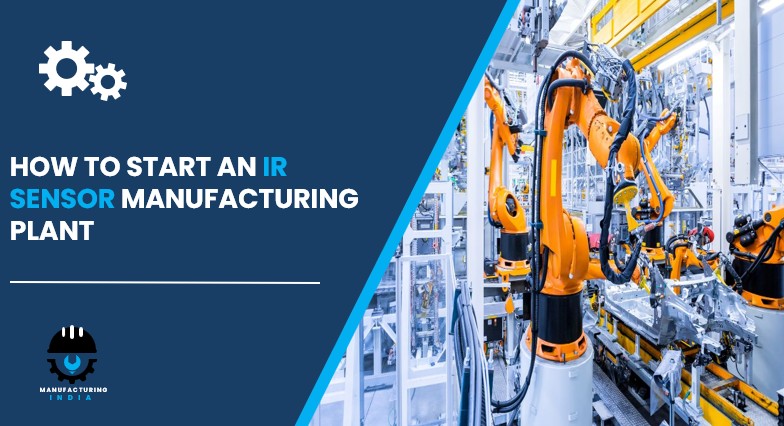
Setting up an IR sensor manufacturing plant in India represents a highly attractive investment proposition underpinned by robust and structurally growing demand from consumer electronics manufacturers, automotive safety system integrators, industrial automation firms, and the expanding Internet of Things (IoT) and smart home device ecosystem. As global electronics production scales, vehicle safety mandates tighten, and industrial process monitoring becomes increasingly automated, infrared (IR) sensors capable of accurately detecting infrared radiation for proximity sensing, motion detection, temperature measurement, and gas analysis occupy an increasingly critical position across consumer, automotive, industrial, and healthcare applications. This growth trajectory, combined with continuous semiconductor miniaturisation and rising demand for contactless sensing technologies, creates a highly favourable manufacturing environment for new entrants with efficient wafer fabrication, packaging, and calibration capabilities.
What is IR Sensor?
An IR sensor is an electronic device that detects infrared radiation emitted or reflected by objects in its field of view and converts it into a measurable electrical signal. IR sensors are broadly classified into active sensors, which emit infrared radiation and measure its reflection, and passive sensors, which detect infrared radiation emitted naturally by objects, and are commonly configured as proximity sensors, motion detectors, thermal sensors, and photodiodes. The manufacturing process begins with semiconductor wafer production, followed by sensing material deposition and photolithography, before proceeding to etching, doping, and chip assembly, culminating in testing and calibration to verify sensitivity, response time, and accuracy.
Beyond their compact form factor, IR sensors are valued for low power consumption and high sensitivity to even minute infrared signals, characteristics that make them well suited to integration into space-constrained consumer devices as well as demanding automotive and industrial environments. The sensors find application across smartphones and wearables, security and surveillance systems, automotive driver assistance systems, industrial process automation, medical devices, and temperature screening equipment.
The global IR sensor market was valued at approximately USD 1.23 Billion in 2025 and is expected to reach USD 2.31 Billion by 2034, exhibiting a CAGR of 7.2% from 2026 to 2034, supported by rising adoption in consumer electronics, growing demand for automation and smart home devices, increasing use in automotive safety systems, and advancements in contactless temperature measurement technologies.
Cost of Setting Up an IR Sensor Manufacturing Plant
The total capital investment required to establish an IR sensor manufacturing plant is shaped by several key parameters: annual production capacity (typically ranging from 5 to 20 million units per annum), the sensor technology mix (active vs. passive sensors, thermopile, pyroelectric, or photodiode-based designs), the level of automation across wafer fabrication, assembly, and testing sections, facility specification, semiconductor-grade cleanroom requirements, and applicable quality and regulatory compliance requirements. Below is a structured breakdown of the major cost components.
1. Capital Expenditure (CapEx)
Total capital investment in an IR sensor manufacturing plant covers the following major heads:
Land and Site Development
This encompasses land acquisition or lease, site preparation, boundary development, and utilities connectivity. Site selection should prioritise proximity to semiconductor material and component suppliers including wafers, lenses, and printed circuit boards (PCBs), as well as access to skilled electronics manufacturing talent. Reliable, high-quality power supply with minimal fluctuation, access to process water for cleanroom humidity and cooling control, strong logistics connectivity for inbound components and outbound finished sensors, and proximity to target electronics, automotive, and industrial customer clusters are critical site selection criteria. Compliance with industrial zoning regulations, semiconductor cleanroom classification standards, electrostatic discharge (ESD) control requirements, and environmental and effluent compliance frameworks must be assessed from project initiation.
Civil Works and Construction
Building costs cover the main production facility including the cleanroom wafer fabrication and thin-film deposition area, photolithography and etching bays, chip dicing and die-attach section, wire bonding and encapsulation area, automated testing and calibration laboratory, packaging and dispatch infrastructure, quality control laboratory, administrative block, and utility infrastructure including power backup, HVAC and cleanroom climate control systems, deionised water systems, and effluent treatment plant. Construction must comply with applicable factory act requirements, cleanroom classification standards (such as ISO 14644), fire and electrical safety norms, and industry quality certification infrastructure guidelines.
Machinery and Equipment
Machinery represents the single largest CapEx component. Key equipment required for an IR sensor manufacturing plant includes:
- Wafer Fabrication Systems: Semiconductor wafer processing equipment for substrate preparation, cleaning, and initial surface conditioning prior to sensing material deposition
- Thin Film Deposition Equipment: Physical and chemical vapour deposition systems for depositing sensing materials and thin-film layers onto semiconductor substrates with precise thickness control
- Photolithography Equipment: Mask aligners and exposure systems for patterning circuit and sensor geometries onto coated wafers with micron-level precision
- Etching Systems: Wet and dry etching equipment for selectively removing material to define sensor structures and circuit patterns following photolithographic patterning
- Doping and Diffusion Furnaces: Equipment for introducing dopants into semiconductor substrates to establish the electrical characteristics required for sensor functionality
- Wafer Dicing Saws: Precision dicing equipment for cutting processed wafers into individual sensor die while minimising chipping and material loss
- Die Bonding Systems: Automated die-attach equipment for mounting diced sensor chips onto substrates or lead frames with accurate placement and adhesive curing
- Wire Bonding Machines: Fine-wire bonding equipment for creating electrical interconnections between sensor die and package leads
- Encapsulation Systems: Moulding and encapsulation equipment for protecting sensor die from moisture, dust, and mechanical damage while maintaining optical window clarity for infrared transmission
- Automated Testing and Calibration Equipment: Functional test systems for verifying sensitivity, response time, signal-to-noise ratio, and calibration accuracy of finished sensors under controlled conditions
- Quality Control Laboratory Equipment: Equipment for optical, electrical, and reliability testing including thermal cycling, humidity testing, and accelerated life testing to verify compliance with industry quality standards
- Automated Packaging Lines: Tape-and-reel, tray, and tube packaging systems for finished sensor units, along with labelling and traceability marking equipment for shipment to electronics assemblers
Other Capital Costs
These include pre-operative expenses, commissioning charges, import duties on specialised semiconductor processing and testing equipment, staff training and competency development, initial raw material and consumable inventory for production commissioning, cleanroom certification and qualification costs, and quality management system establishment costs including ISO 9001 and applicable automotive or industrial quality standards.
Request a Sample Report for In-Depth Market Insights: https://www.imarcgroup.com/ir-sensor-manufacturing-plant-project-report/requestsample
2. Operational Expenditure (OpEx)
Raw materials principally semiconductor materials, lenses, and printed circuit boards (PCBs) constitute the dominant operating cost, typically representing 60–70% of total OpEx. Utility costs, driven primarily by cleanroom HVAC operation, electricity consumption of deposition and testing equipment, and deionised water systems, account for 10–15% of OpEx. Labour, maintenance, quality control, packaging, transportation, depreciation, taxes, and overhead costs constitute the remainder of the operating cost base.
3. Plant Capacity
The proposed IR sensor manufacturing facility is designed with an annual production capacity ranging between 5–20 million units, enabling economies of scale while maintaining operational flexibility. This capacity range supports a diversified product portfolio spanning active and passive IR sensors including proximity sensors, motion detectors, thermal sensors, and photodiodes, serving consumer electronics, automotive, industrial automation, and healthcare device customers.
4. Profit Margins and Financial Projections
The project demonstrates healthy profitability potential under normal operating conditions. Financial projections encompass capital investment, operating costs, capacity utilisation ramp-up schedule, product mix across sensor types, and forward demand outlook underpinned by rising automation and smart device adoption. A comprehensive feasibility analysis includes sensitivity analysis, Net Present Value (NPV), Internal Rate of Return (IRR), and Payback Period calculations. Gross profit margins for IR sensor manufacturing typically range from 40–50%, supported by stable demand, high value-added applications, and efficient production scale. Net profit margins of 20–28% are achievable with disciplined cost management, optimal capacity utilisation, and effective yield management across the wafer fabrication and assembly process.
Why Set Up an IR Sensor Manufacturing Plant?
Growth in Smart Devices and IoT Integration
Expanding adoption of Internet of Things (IoT) and connected devices is increasing sensor integration across consumer electronics, smart home systems, and wearable devices. As smartphones, tablets, and wearables increasingly rely on proximity sensing and gesture-based interaction, IR sensors are transitioning from a specialised component toward a standard feature across a widening range of consumer electronics categories, supporting steady volume growth.
Automotive Technology Advancements
Rising demand for safety and driver assistance features is driving increased integration of infrared sensing technologies into advanced driver assistance systems (ADAS) and cabin monitoring applications. As automotive manufacturers incorporate infrared sensing into driver monitoring, occupancy detection, and safety systems, IR sensors are becoming an increasingly standard component of modern vehicle architectures, supporting sustained industrial demand.
Contactless Technology Trend
Increasing reliance on touchless detection systems across consumer, healthcare, and industrial settings enhances market opportunities for IR sensors. Advancements in contactless temperature measurement and non-contact process monitoring technologies are broadening the addressable applications for infrared sensing beyond traditional proximity and motion detection use cases.
Industrial Automation Expansion
Automation across manufacturing sectors is driving sensor demand as industrial facilities adopt non-contact measurement tools for improved process efficiency and accuracy. According to industry estimates, the median share of industrial manufacturers with highly automated processes is projected to more than double, increasing from 18% to 50%, supporting sustained industrial demand for IR sensors used in process monitoring and control applications.
High Value-Added Electronics Segment
IR sensors represent a specialised semiconductor product category offering attractive margins relative to commodity electronic components. The technical complexity of wafer fabrication, thin-film deposition, and precision calibration creates meaningful barriers to entry, supporting favourable pricing dynamics for manufacturers with established process capability and quality certification.
Diversified End-Use Base Across Multiple Industries
IR sensors serve a structurally diversified customer base spanning consumer electronics manufacturers, automotive companies, industrial automation firms, healthcare device producers, security system providers, and IoT solution developers. This diversification provides resilience against single-segment demand volatility while allowing manufacturers to balance production across multiple end-use verticals.
Manufacturing Process Overview
The IR sensor manufacturing process transforms raw semiconductor wafers into calibrated, packaged sensing devices through a sequence of fabrication, assembly, and testing operations. The key process stages are:
- Wafer Fabrication: Semiconductor wafers are processed and prepared as the base substrate for sensor construction, with surface cleaning and conditioning performed to ensure defect-free deposition in subsequent steps
- Thin Film Deposition: Sensing materials are deposited onto the wafer surface using physical or chemical vapour deposition techniques, forming the infrared-sensitive layers that convert incident radiation into electrical signals
- Photolithography: Light-sensitive photoresist is applied and selectively exposed to define the circuit and sensor element patterns that will be transferred onto the wafer in subsequent etching steps
- Etching: Wet or dry etching processes selectively remove material according to the photolithographic pattern, defining the sensor structures and interconnecting circuitry on the wafer
- Doping: Dopant materials are introduced into targeted regions of the semiconductor substrate to establish the electrical properties required for sensor operation
- Wafer Dicing: Processed wafers are cut into individual sensor die using precision dicing saws, with careful process control to minimise chipping and material loss
- Die Bonding: Individual sensor die are mounted onto substrates or lead frames using precision die-attach equipment, with adhesive curing to secure mechanical and thermal contact
- Wire Bonding: Fine wires are bonded between the sensor die and package leads to establish electrical interconnections
- Encapsulation: Sensor assemblies are encapsulated to protect against moisture, dust, and mechanical damage, while preserving an optical window for infrared transmission to the sensing element
- Calibration: Encapsulated sensors are calibrated against reference standards to establish accurate sensitivity, response, and output characteristics
- Functional Testing: Finished sensors undergo functional testing to verify sensitivity, response time, signal-to-noise ratio, and compliance with product specifications before release
- Packaging and Dispatch: Qualified sensors are packed in tape-and-reel, tray, or tube formats appropriate for automated pick-and-place assembly by electronics manufacturers, and dispatched to consumer electronics, automotive, and industrial customers
Key Applications of IR Sensor
- Consumer Electronics: IR sensors are embedded in smartphones, tablets, and wearables to detect proximity and enable gesture-based interactions, supporting features such as automatic screen dimming and touchless controls
- Automotive Systems: Utilised in advanced driver assistance systems (ADAS) and cabin monitoring applications for improved safety and comfort, including driver attention monitoring and occupancy detection
- Industrial Automation: Applied for non-contact temperature measurement and process control to enhance efficiency and accuracy across manufacturing and process industries
- Security and Surveillance: Integrated into motion detection and alarm systems to enhance security and prevent unauthorised access across residential, commercial, and industrial premises
- Healthcare and Medical Devices: Used in contactless temperature screening equipment and medical monitoring devices requiring accurate, non-invasive infrared measurement
- Smart Home Automation: Incorporated into occupancy sensors, smart lighting controls, and home security systems supporting the expanding smart home device ecosystem
Global IR Sensor Market Outlook
The global IR sensor market was valued at approximately USD 1.23 Billion in 2025. According to IMARC Group estimates, the market is expected to reach USD 2.31 Billion by 2034, exhibiting a CAGR of 7.2% from 2026 to 2034. The IR sensor market benefits from multiple structural demand drivers:
- Rising adoption of IR sensors in consumer electronics including smartphones, tablets, and wearable devices for proximity sensing and gesture-based interaction
- Growing demand for automation and smart home devices, supporting expanded sensor integration across occupancy, lighting, and security applications
- Increasing use of infrared sensing technologies in automotive safety systems, including advanced driver assistance systems and cabin monitoring applications
- Expansion of industrial process monitoring, with manufacturers adopting non-contact measurement tools to improve efficiency and reduce downtime
- Advancements in contactless temperature measurement technologies, broadening application across healthcare, industrial, and consumer settings
- Continued semiconductor industry investment in manufacturing process development, product miniaturisation, and energy-efficient sensor technologies
- Expanding smart infrastructure and IoT connectivity, supporting sustained sensor demand across residential, commercial, and industrial installations
Major players in the global IR sensor manufacturing industry include FLIR Systems, Inc., Hamamatsu Photonics K.K., Murata Manufacturing Co., Ltd., Texas Instruments Incorporated, Raytheon Technologies Corporation, Honeywell International Inc., NXP Semiconductors N.V., and Teledyne Technologies Incorporated, serving end-use sectors including consumer electronics manufacturers, automotive companies, industrial automation firms, healthcare device producers, security system providers, and IoT solution developers.
Latest Industry Developments
- February 2026: Boeing expanded production capacity for electro-optical/infrared (EO/IR) satellite sensors through a new manufacturing facility, incorporating modular assembly, advanced cleanrooms, and automated equipment to scale output for missile warning and tracking applications, alongside digital engineering and supply chain resilience improvements supporting large-scale space asset production.
- August 2025: L3Harris Technologies began production of EO/IR sensor systems at a newly established facility spanning approximately 2,000 square metres in Katowice, Poland, producing sensors for intelligence, surveillance, reconnaissance, and targeting applications, with plans to expand production capacity and delivery capability supporting European security operations.
Licenses and Regulatory Requirements
Establishing an IR sensor manufacturing unit requires a range of approvals and certifications, which may vary by country and jurisdiction, including:
- Business registration and company incorporation under applicable company law
- Factory License under applicable state Factories Act provisions for manufacturing operations
- Electronics and semiconductor manufacturing registration where applicable under national industrial policy frameworks
- ISO 9001:2015 Quality Management System Certification for quality management infrastructure compliance
- ISO 14001 Environmental Management System Certification for environmental compliance
- IATF 16949 certification where sensors are supplied to automotive customers, covering automotive quality management requirements
- ISO 14644 cleanroom classification compliance for semiconductor-grade production environments
- Pollution Control Board Clearances Consent to Establish (CTE) and Consent to Operate (CTO) for manufacturing operations
- Hazardous waste handling and disposal compliance for semiconductor process chemicals and consumables
- Electrical safety and product certification compliance including RoHS and REACH where applicable for export markets
- Export-Import Code (IEC) for international market access
- Trademark and Brand Registration for proprietary branded product launch
- Occupational Health and Safety management compliance (ISO 45001 / Factories Act provisions) for manufacturing worker safety in cleanroom and chemical handling areas
Key Challenges to Consider
Raw Material Supply Consistency and Semiconductor Material Costs
Semiconductor materials, which account for 60–70% of total operating costs, are subject to global supply chain dynamics, pricing volatility, and periodic shortages affecting the broader electronics industry. Securing long-term supply agreements with semiconductor material, lens, and PCB suppliers, and maintaining diversified sourcing relationships, are critical operational priorities to manage input cost and availability risk.
Cleanroom and Process Technology Investment
IR sensor fabrication requires precise cleanroom environments and advanced process technology for deposition, photolithography, and etching operations. Any lapse in cleanroom classification maintenance or process control increases defect rates and yield loss, directly affecting production economics. Continuous investment in equipment maintenance, process qualification, and cleanroom certification compliance is a non-negotiable operational requirement.
Technology Evolution and Product Obsolescence Risk
The semiconductor sensor industry is characterised by continuous technological advancement, including product miniaturisation and improvements in sensitivity and power efficiency. Manufacturers must sustain ongoing investment in process development and product innovation to avoid technology obsolescence and maintain competitiveness against evolving customer specifications and emerging sensor technologies.
Quality Certification and Automotive/Industrial Compliance Maintenance
Maintaining ISO quality certifications, automotive IATF 16949 compliance where applicable, and consistent product reliability across all production batches requires disciplined process control and rigorous testing infrastructure, as any quality compliance lapse can disrupt customer qualification status and damage long-term commercial relationships, particularly in automotive and industrial customer segments with stringent qualification requirements.
Frequently Asked Questions (FAQs)
1. How much does it cost to set up an IR sensor manufacturing plant?
The total investment depends on plant capacity (5–20 million units per annum), sensor technology mix, automation level, facility specification, location, and target market certifications. Costs cover land, civil construction (cleanroom fabrication area, assembly and testing sections, quality laboratory, utilities), machinery (wafer fabrication, deposition, photolithography, etching, dicing, bonding, encapsulation, and testing equipment), quality certifications, working capital, and regulatory compliance. A comprehensive feasibility study from IMARC Group provides detailed, capacity-specific cost estimates covering all CapEx and OpEx components.
2. Is IR sensor manufacturing a profitable business in 2026?
Yes. Sustained demand from consumer electronics, automotive safety systems, and industrial automation sectors, combined with gross margins of 40–50% and net profit margins of 20–28%, make IR sensor manufacturing financially attractive. The specialised, high value-added nature of infrared sensing technology supports favourable pricing dynamics relative to commodity electronic components.
3. What machinery and equipment are required for an IR sensor manufacturing plant?
Key equipment includes wafer fabrication systems, thin film deposition equipment, photolithography systems, wet and dry etching equipment, doping and diffusion furnaces, wafer dicing saws, die bonding systems, wire bonding machines, encapsulation systems, automated testing and calibration equipment, and automated packaging lines for tape-and-reel, tray, and tube formats.
4. What licenses and approvals are required?
Required approvals include company registration, Factory License, ISO 9001:2015 Quality Management System certification, ISO 14001 Environmental Management System certification, IATF 16949 certification for automotive customers where applicable, cleanroom classification compliance, Pollution Control Board clearances, and product certifications including RoHS and REACH for export markets.
5. How long does it take to commission an IR sensor manufacturing plant?
Typically, 12–24 months from project initiation to commercial production launch, depending on project scale, cleanroom construction timeline, equipment procurement lead times for semiconductor fabrication and testing systems, process qualification, and quality certification timelines, which should be initiated early in the project to avoid delays to commercial launch.
6. What are the key raw materials for IR sensor manufacturing?
The primary raw materials are semiconductor materials used for wafer substrates and sensing layers, along with lenses for optical focusing and printed circuit boards (PCBs) for sensor assembly and interconnection. Other key inputs include bonding wire, encapsulation compounds, and packaging materials for finished sensor dispatch.
7. What is the break-even period for an IR sensor manufacturing plant?
The break-even period generally depends on capacity utilisation ramp-up trajectory, the product mix across active and passive sensor types, customer qualification timelines particularly for automotive and industrial customers, and yield performance across the wafer fabrication and assembly process. Securing long-term supply agreements and stable customer offtake arrangements significantly improves revenue predictability and supports faster break-even achievement.
8. What are the main types of IR sensors and their applications?
The two principal categories are active sensors, which emit infrared radiation and measure its reflection for proximity and distance sensing, and passive sensors, which detect infrared radiation emitted naturally by objects for thermal and motion sensing applications. Common configurations include proximity sensors, motion detectors, thermal sensors, and photodiodes, serving consumer electronics, automotive, industrial, security, and healthcare applications.
9. What government incentives are available for IR sensor manufacturers?
Manufacturers may benefit from electronics and semiconductor manufacturing incentive schemes, production-linked incentive (PLI) programmes supporting domestic electronics component manufacturing, state-level industrial investment incentives and capital subsidies, and export promotion benefits for semiconductor and sensor product exports. Evolving national semiconductor policy frameworks also affect the economics of establishing new sensor fabrication capacity.
10. How does IR sensor manufacturing compare to other semiconductor sensor manufacturing in terms of setup?
Compared to other semiconductor sensor categories, IR sensor manufacturing shares broadly similar wafer fabrication, photolithography, and packaging technology, allowing manufacturers with experience in semiconductor processing to adapt existing technical capabilities to IR sensor production with targeted investment in infrared-specific sensing material deposition and optical packaging infrastructure. However, IR sensors require additional process control for optical window integrity and infrared transmission characteristics not required for non-optical sensor types.
Key Takeaways for Investors
The IR sensor manufacturing industry represents a structurally resilient and financially attractive investment opportunity positioned at the intersection of expanding consumer electronics production, tightening automotive safety mandates, and accelerating industrial automation adoption. Stable demand from consumer electronics, automotive, industrial automation, security, and healthcare channels provides resilience against single-segment demand volatility, while the specialised, high value-added nature of infrared sensing technology supports attractive margin potential relative to commodity electronic components. Continued semiconductor industry investment in miniaturisation and energy-efficient sensor technologies, combined with expanding IoT and smart infrastructure deployment, provides a structural demand tailwind for new entrants with efficient wafer fabrication, packaging, and calibration capabilities. The scalable nature of the sensor manufacturing value chain allows investors to phase capital deployment according to risk appetite and target market positioning, while continued investment by established sensor manufacturers in expanding production capacity reflects strong confidence in the long-term growth and profitability of the category.
About the Author